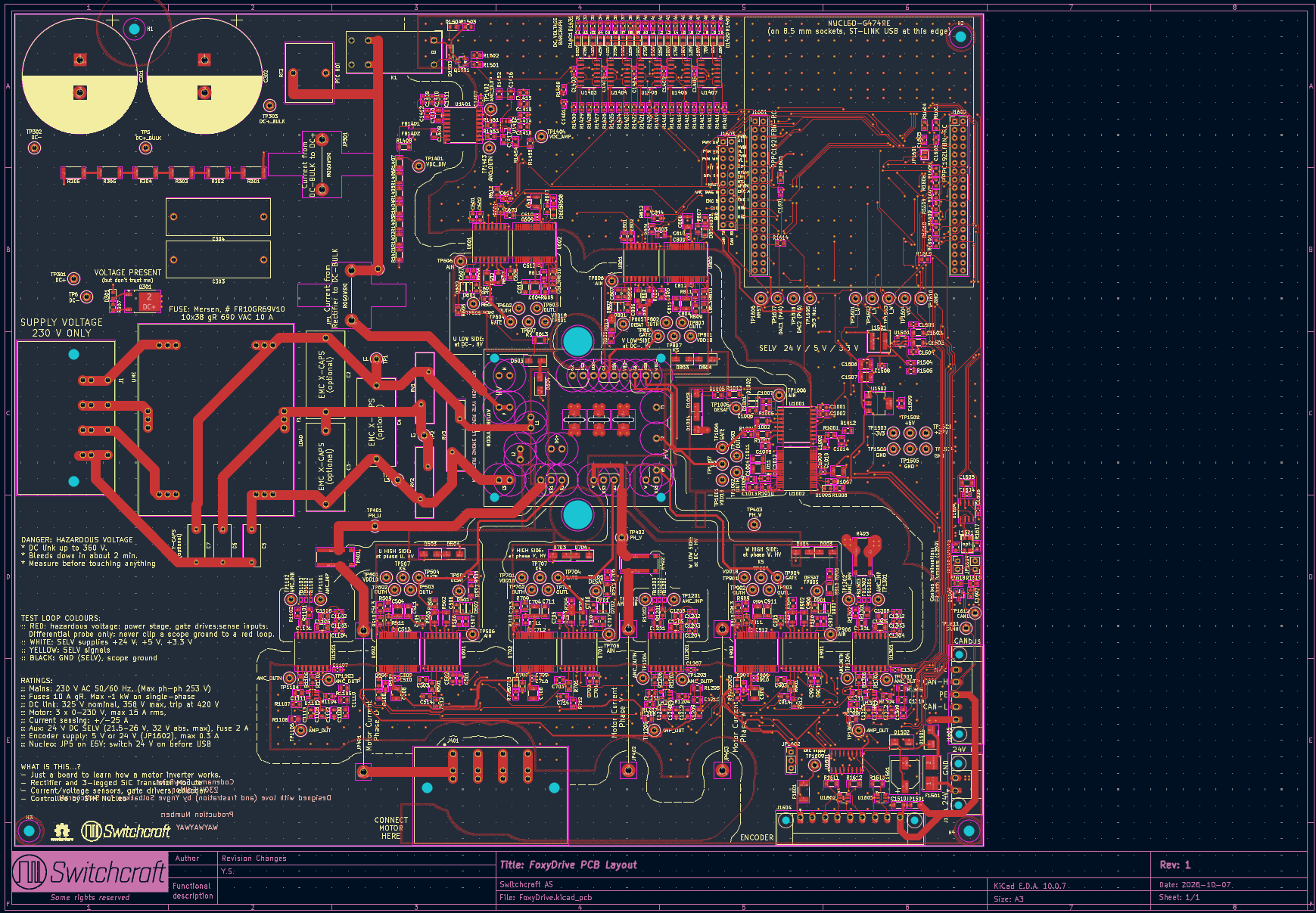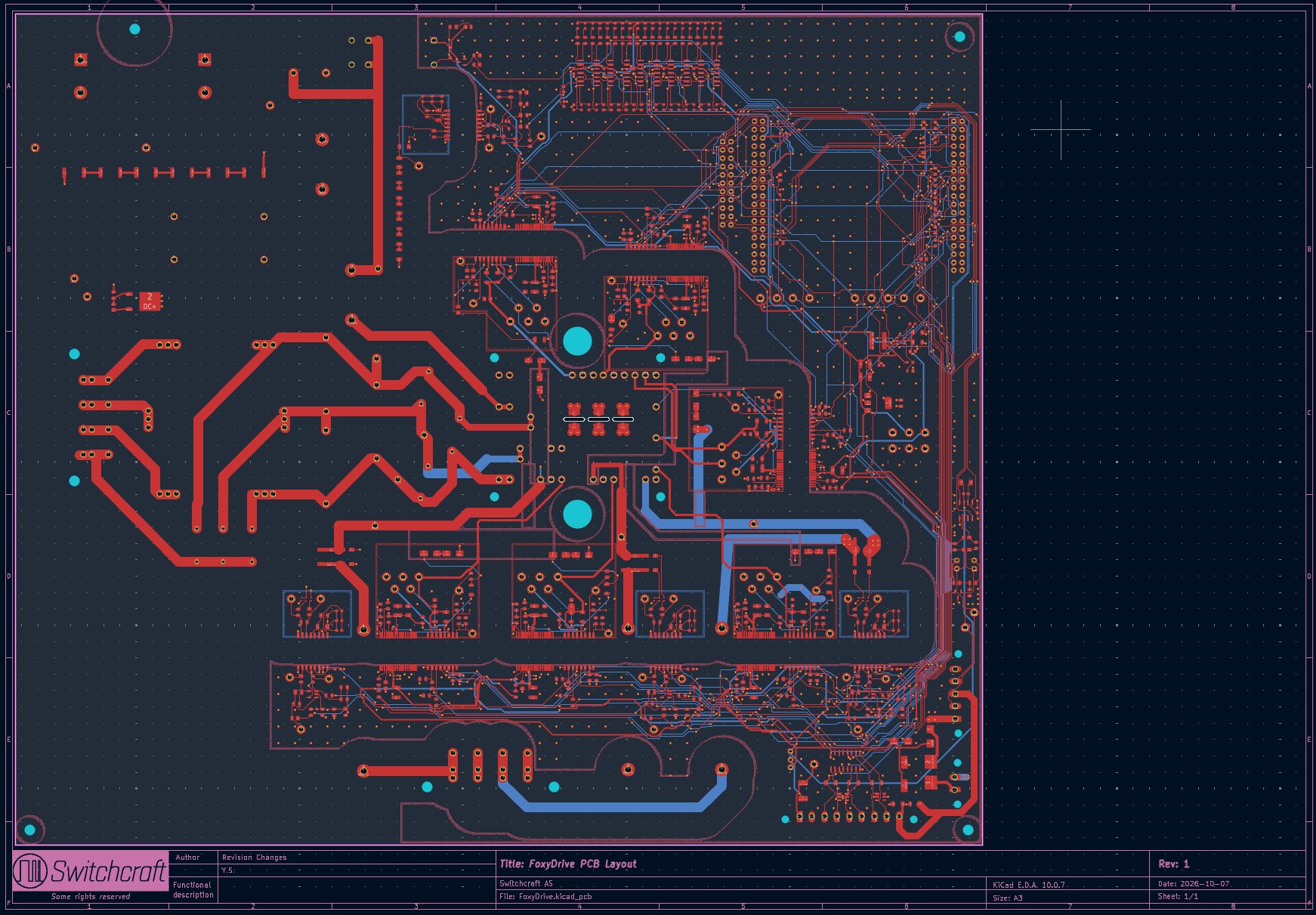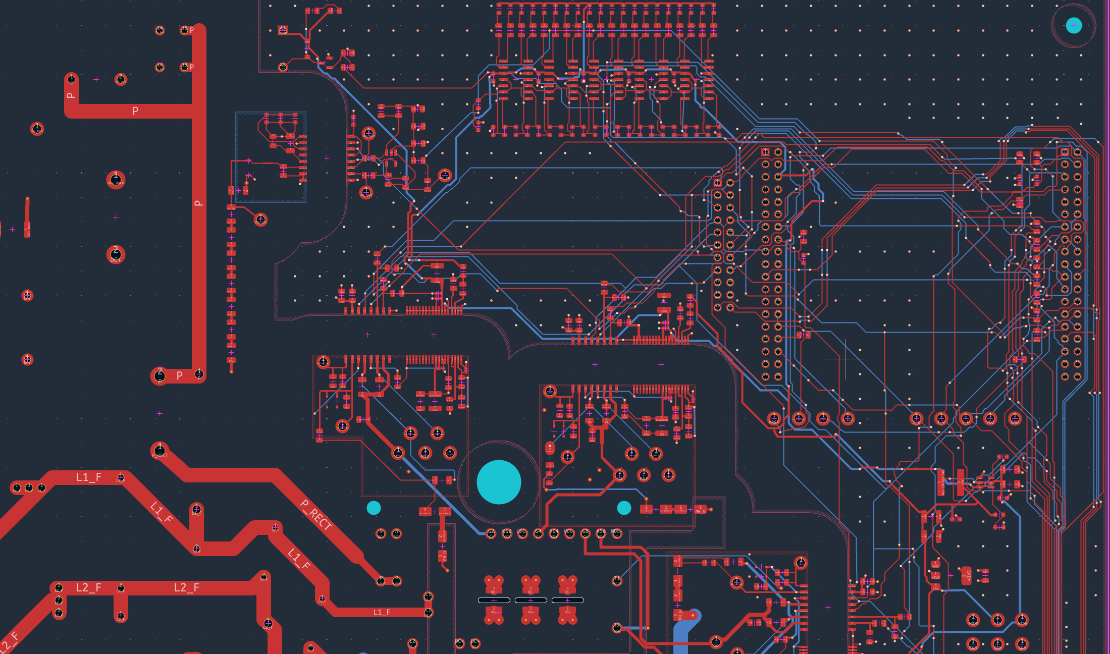
Finally, some switchcrafting
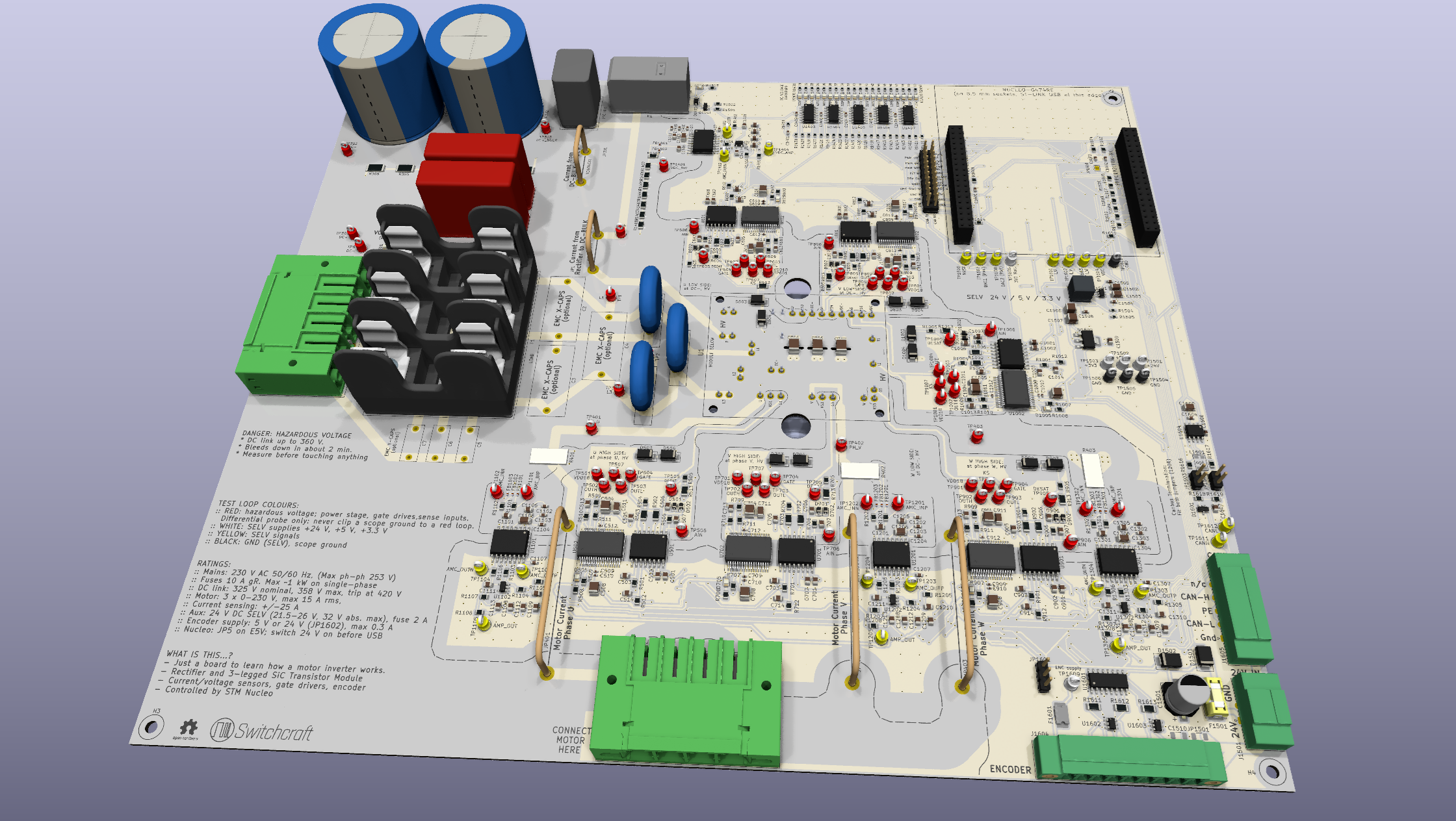
It has taken quite a while.
My previous update on the inverter card is little over 8 years ago. Life happened, and then I never really got all the PCB traces to reach their components without clashing into each other because I was too cheap to invest in a four-layer stack up.
So I evaluated that entire board and basically started from scratch:
Goal
Generally, we can sort learning into two methods:
Read about other people’s explanations and experiences and use that to build your own understanding
Create your own experiences and take learning directly from that
I am a big proponent of the latter. I learn when i see what is going in with my own eyes. When I fuck up some thing or when I finally get something up and running.
So I decided that to really boost my understanding about motor drives, I must stop reading about it and start doing it.
The goals is therefore
to build a complete motor drive where one can measure everything. Not just the motor current and DC-link voltage, but also the complete gatedriver chain, the measurement chains, the PWM outputs, the flow of current between different stages of the DC link and so forth.
Result
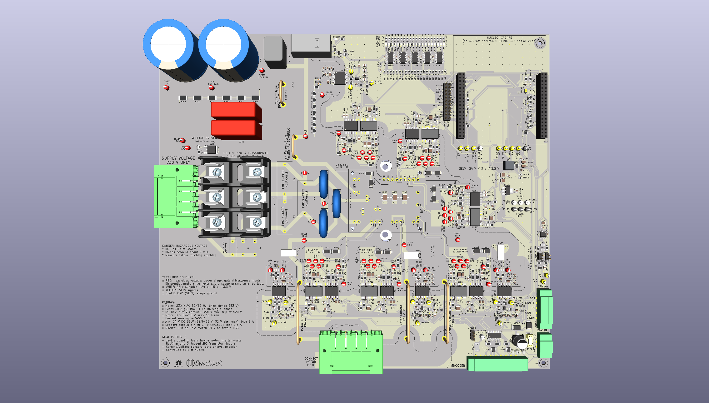
It is a complete redesign of the 2018 version:
Gate drivers and measurement circuits are on the same board as the power electronics
Real isolation distances: 8 mm between low voltage (SELV) and high voltage traces, even if they are on separate layers
A proper precharge circuit (which I didn’t even have in 2018)
Stacked DC planes instead of DC+ and DC- side by side
Isolated ICs rated for common-mode edges from SiC switching at 85-150 kV/µs (even though the actual SiC switches at 30 kV/µs)
The board’s main purpose is that every interesting node should be easy to measure with an Oscilloscope
Plans (sorted by ambition)
Get the card manufactured and assembled
Perform bring-up testing to assess switching performance, isolation, functionality etc.
Create a program that runs an induction motor with open loop scalar control (V/f)
Field-oriented control
Write a program that runs test on the motor to identify motor parameters (ID-run)
Experiments:
Switching techniques
Dead-time compensation
Gate-resistor and dV/dt studies
EMC-testing (common mode, reflection, measures which affects EMC and common-mode content)
Load bench testing with brake-testing against another motor
Later, a revised board, V2, will be designed based on these experiments where higher voltage and output rating is targeted.
Functions and features
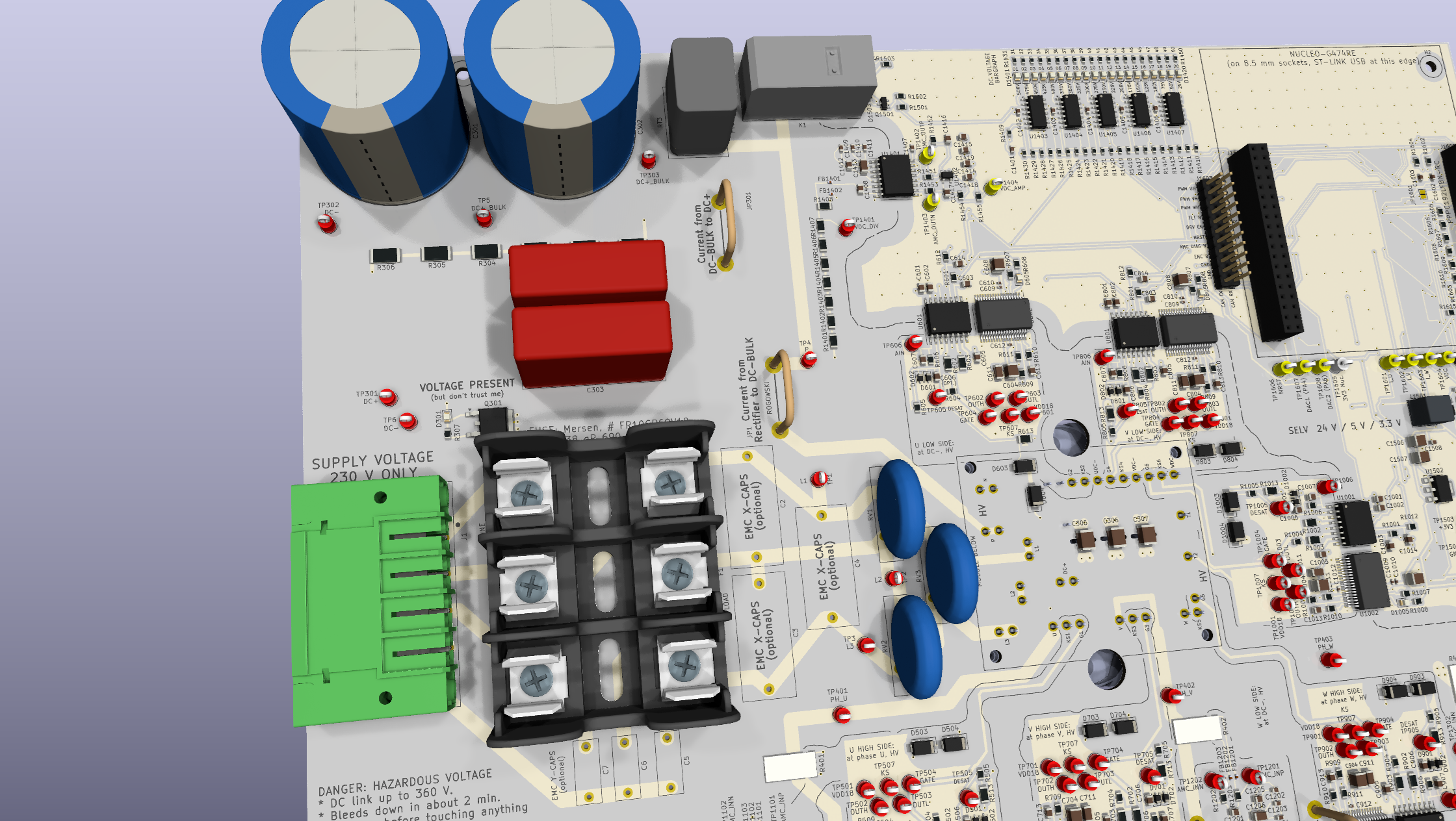
As the board is designed to be a learning-board, it is designed to run on single-phase 230 V 50/60 Hz. I want to be able to sit in my living room with my card, not needing a three-phase outlet which most people doesn’t have indoors at all. It does work with three phases however, but it also works fine on single phase. The capacitor bank design needed some extra care in that respect as rectified single phase has an awful long dip between the peaks compared to rectified three-phase.
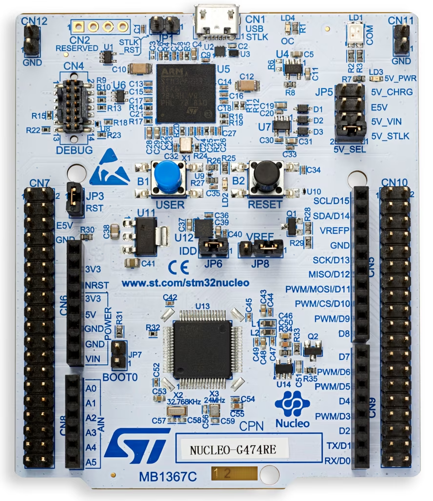
A STM32 Nucleo board is used to gather measurements and provide PWM signals to the gate drivers. Some of its internal comparators are used for hardware protection. More about this board later.
Further specs:
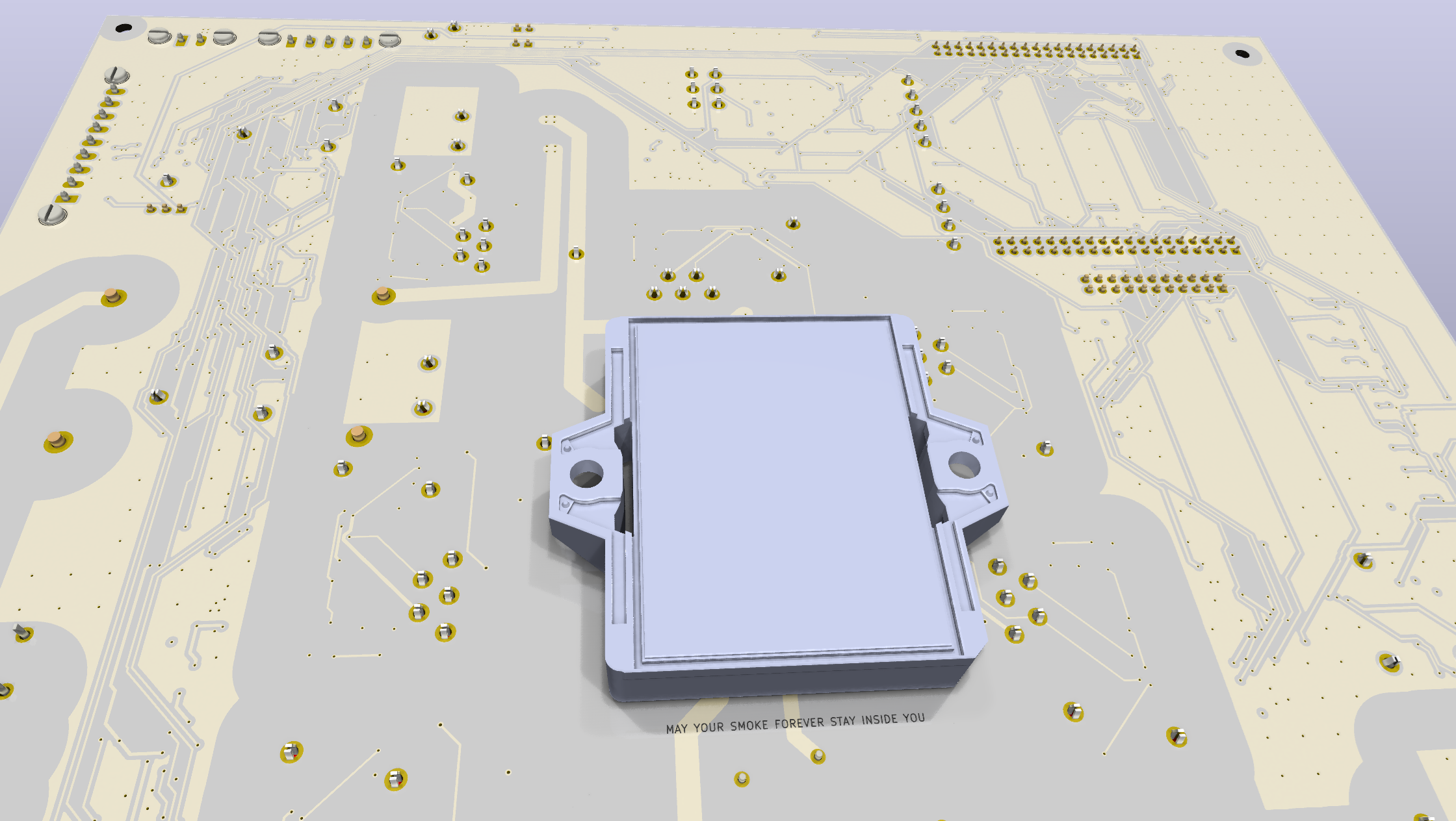
SiC Module: Semikron SEMITOP E2 with a 3-phase rectifier and a 1200 V SiC MOSFET six-pack in one package. The module is rated 29 A
The rest of the power stage is designed for 15 A rms (about 21 A peak)
Input chain:
Plug for 230 V mains.
gR-semiconductor fuses.
Surge varistors.
Footprints ready for EMC-components (X- and Y-capacitors) which will be fitted later.
Precharge: A PTC inrush limiter which is bypassed by a relay once the DC-link voltage has reached a sufficient level.
DC-link:
1360 µF electrolytic capacitors for energy storage (this is a lot, but needed to create a buffer between the single-phase peaks).
Film-capacitors and ceramics placed close to the switches to accommodate fast edges.
Stacked DC- and DC+ planes, helps to keep stray inductance low.
Bleeder circuit to discharge the link in a little under 2 minutes.
Gate Drivers
Six isolated gate driver cells (TI UCC21750) - one per switch. Placed close to the SiC module.
Each cell has its own reinforced 18V isolated supply.
0/18V gate drive with Miller clamp.
Separate turn-on and turn-off resistors on footprints which are easy to swap (for dV/dt experiments).
Short-circuit protection: DESAT detection which reacts in about 1 µs with soft turn-off. (The actual SiC switches are rated to withstand a short circuit for 2 µs, so it was required to design a DESAT detection circuit which was faster).
Hardware interlock between each leg so that both switches can never be on at the same time, even if I screw up the firmware.
Isolated measurement/sensing
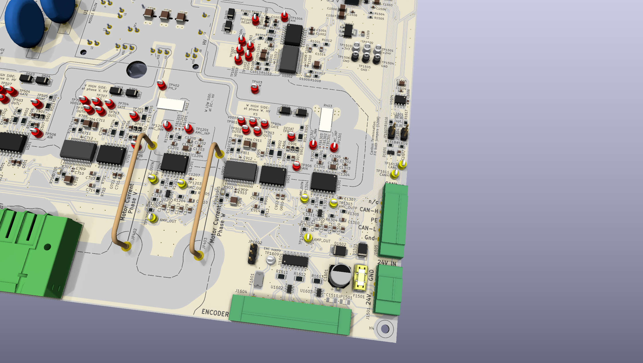
Phase currents are measured using a 4-terminal measurement shunt in each phase. An isolated reinforced amplifier (TI AMC3301) is used to send the measurements to the analog inputs. Range is ±25 A.
DC-link voltage is measured using an isolated amplifier (TI AMC3311) scaled 0-550 V with over voltage trip.
Module temperature: The SiC module has an internal NTC which is read through one gate driver’s isolated analog channel.
Protection
Hardware overcurrent trip on both the high and low limit of each phase. This is achieved by using the STM32’s internal comparators on the Nucleo board. These go straight to the PWM timer’s break input.
DC-link overvoltage trip.
Fault line from all six gate drivers.
DESAT short-circuit protection in every gate driver.
Control
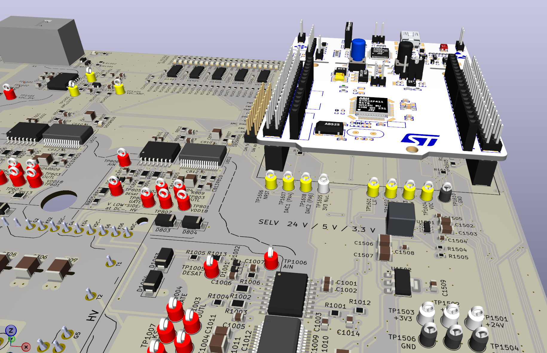
An STM32 NUCLEO-G474RE board plugs directly onto the power board.
Firmware is bare-metal, written at register level.
Current and voltage are sampled at the same instant, synchronised to the PWM.
128 KB of RAM for logging data and streaming to a PC.
Encoder input for industrial incremental encoders (RS-422), for speed feedback while developing/double checking FOC.
CAN / CAN FD interface for a PC or other nodes, with switchable bus termination 120R resistors.
Safety and Isolation
The whole isolation barrier is on the power board, so everything you touch on the controller side is SELV.
Creepage and clearance follow IEC 60664-1, with reinforced insulation between HV and SELV. The rules are checked automatically in the PCB design by a python script.
HV-present LED powered from the DC link itself, so it works with the auxiliary supply off.
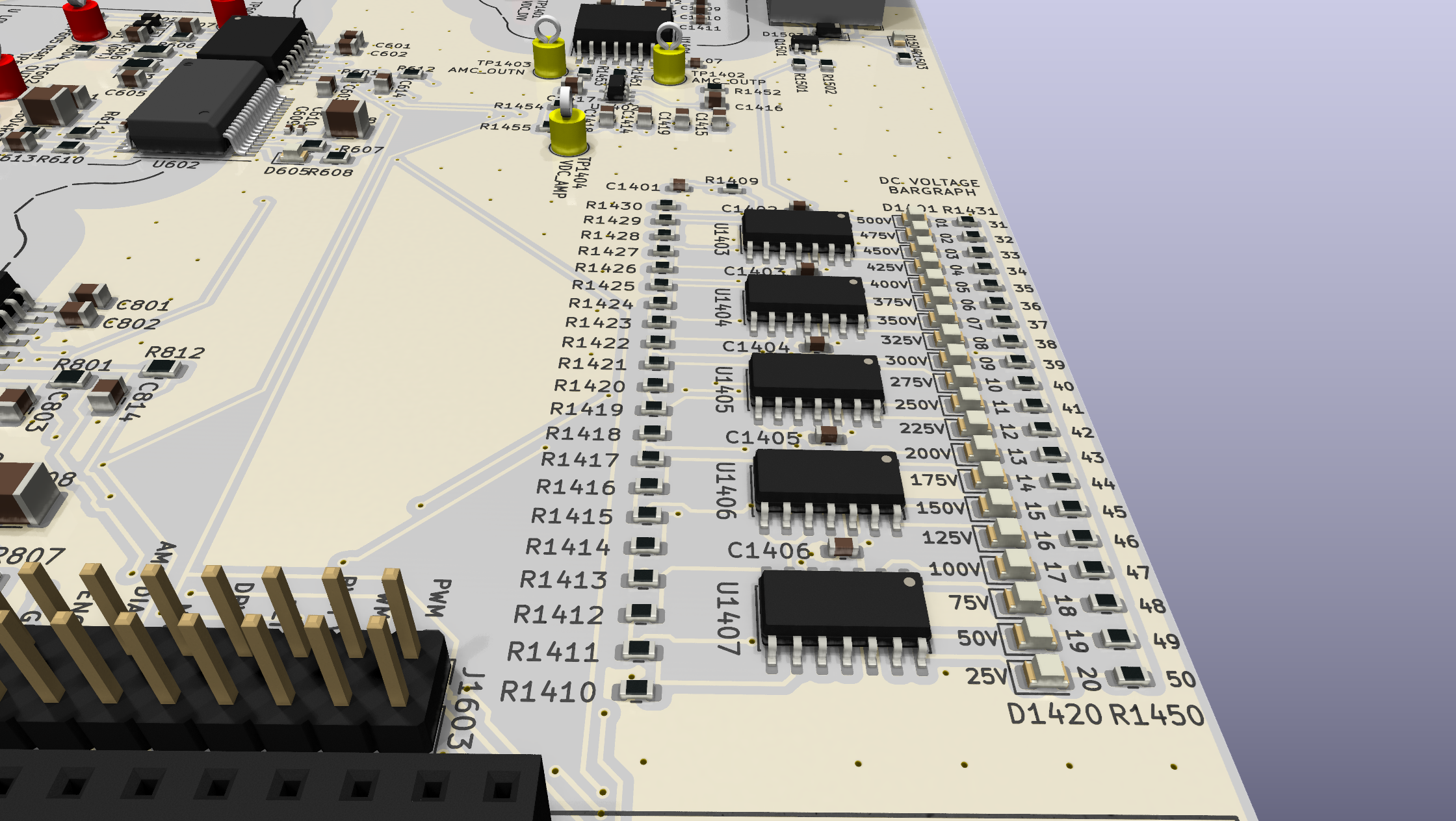
20-LED “bargraph” showing the DC-link voltage, in 25 V steps up to 500 V (I can’t wait to see how this one works).
Auxiliary power comes from an external 24 V SELV supply. Nothing on the board is supplied from the mains apart from the power stage.
Measurement features
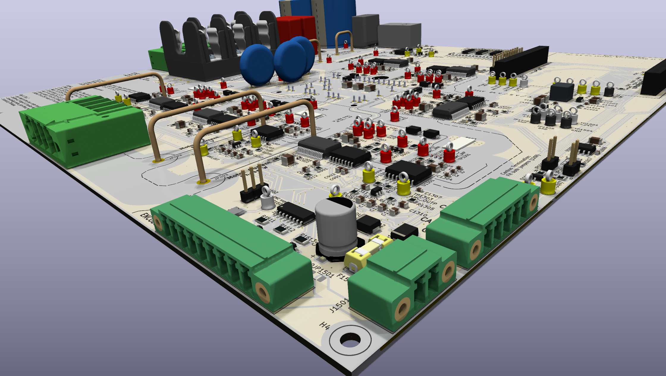
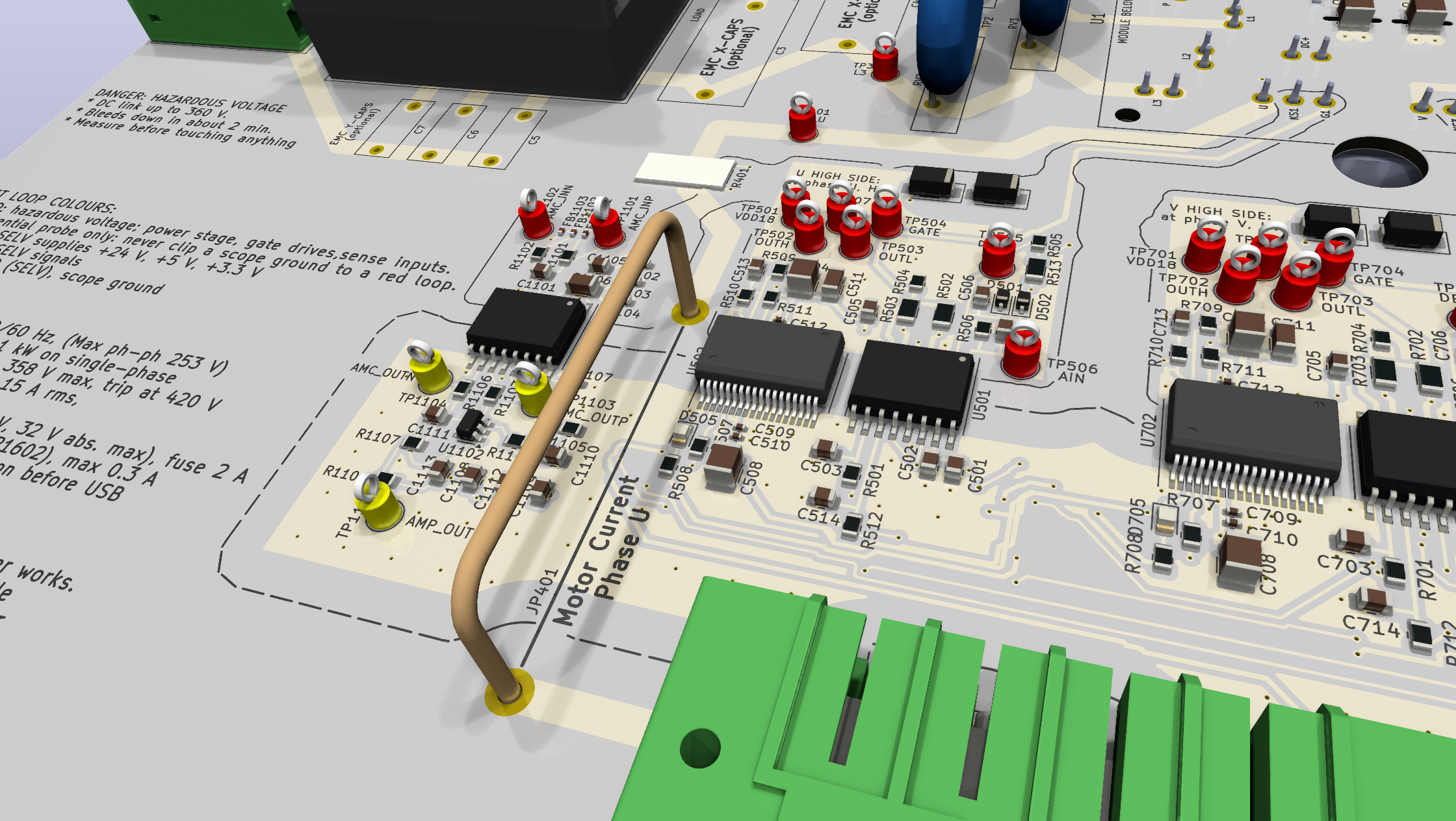
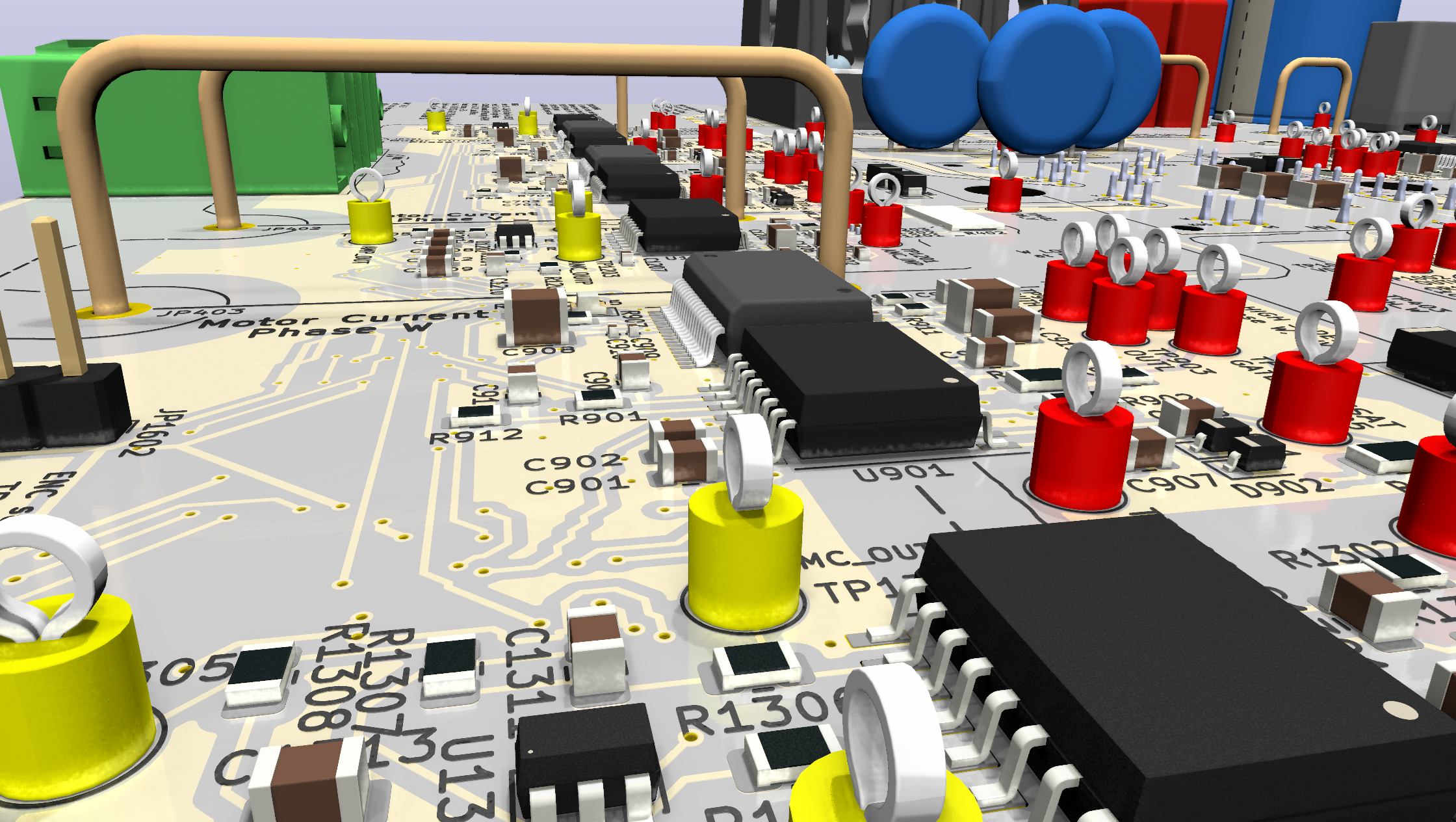
Colour-coded test loops at every stage:
Red: HV and isolated islands (for differential probes only)
Black: GND
White: supply rails
Yellow: signals
Rogowski-coil / current clamp access:
raised wire bridges on all three motor phases
a bridge between the electrolytic bank and the film capacitors, to measure how the ripple current splits.
Gate, driver output, DESAT and supply test points in every gate-driver cell.
Each step of the current and voltage sensing chain can be probed: shunt, isolator output, op-amp and ADC pin.
A 2 × 11 header for a logic analyser: all six PWMs, fault, enable, relay, encoder and CAN.
PCB Board:
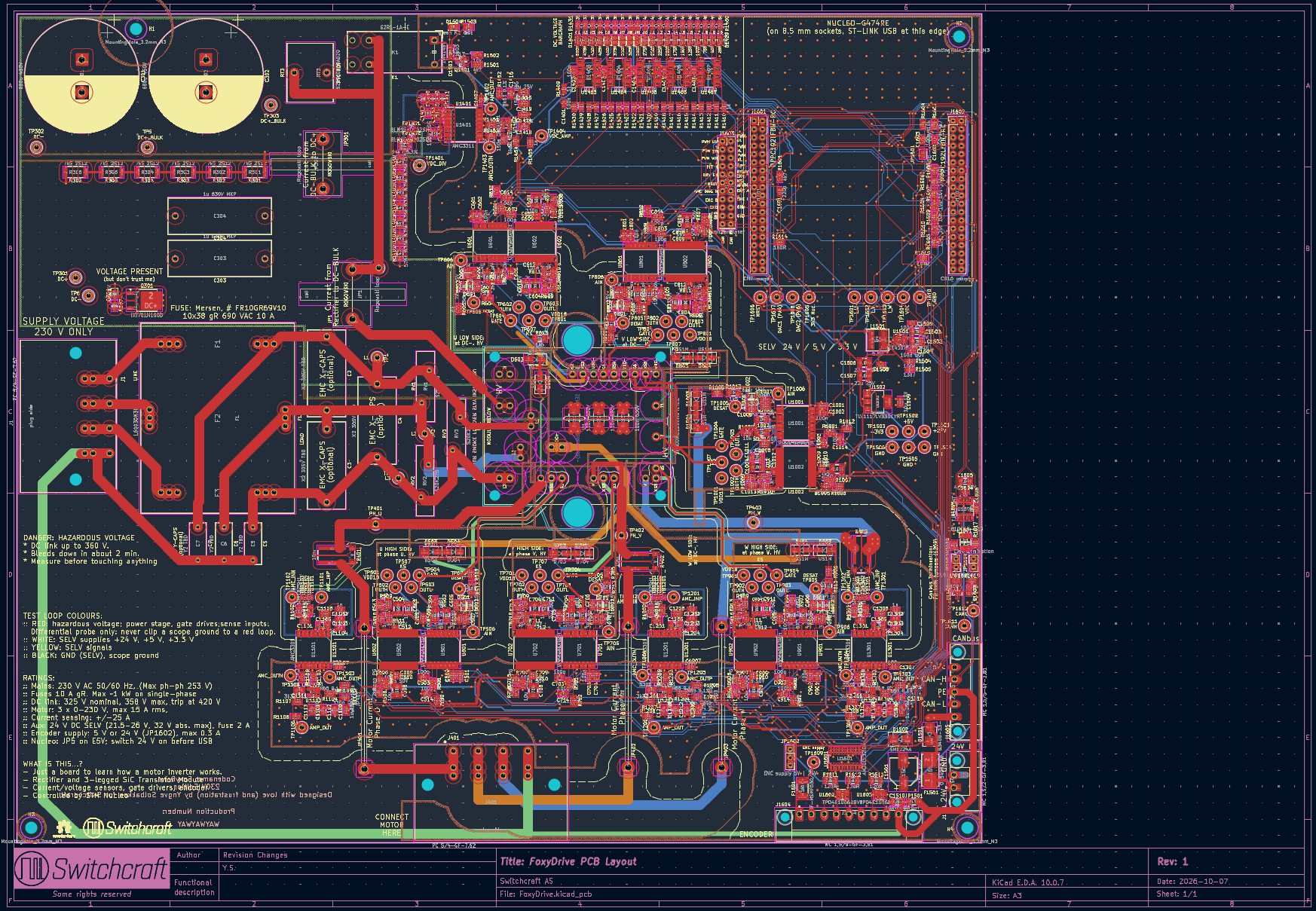
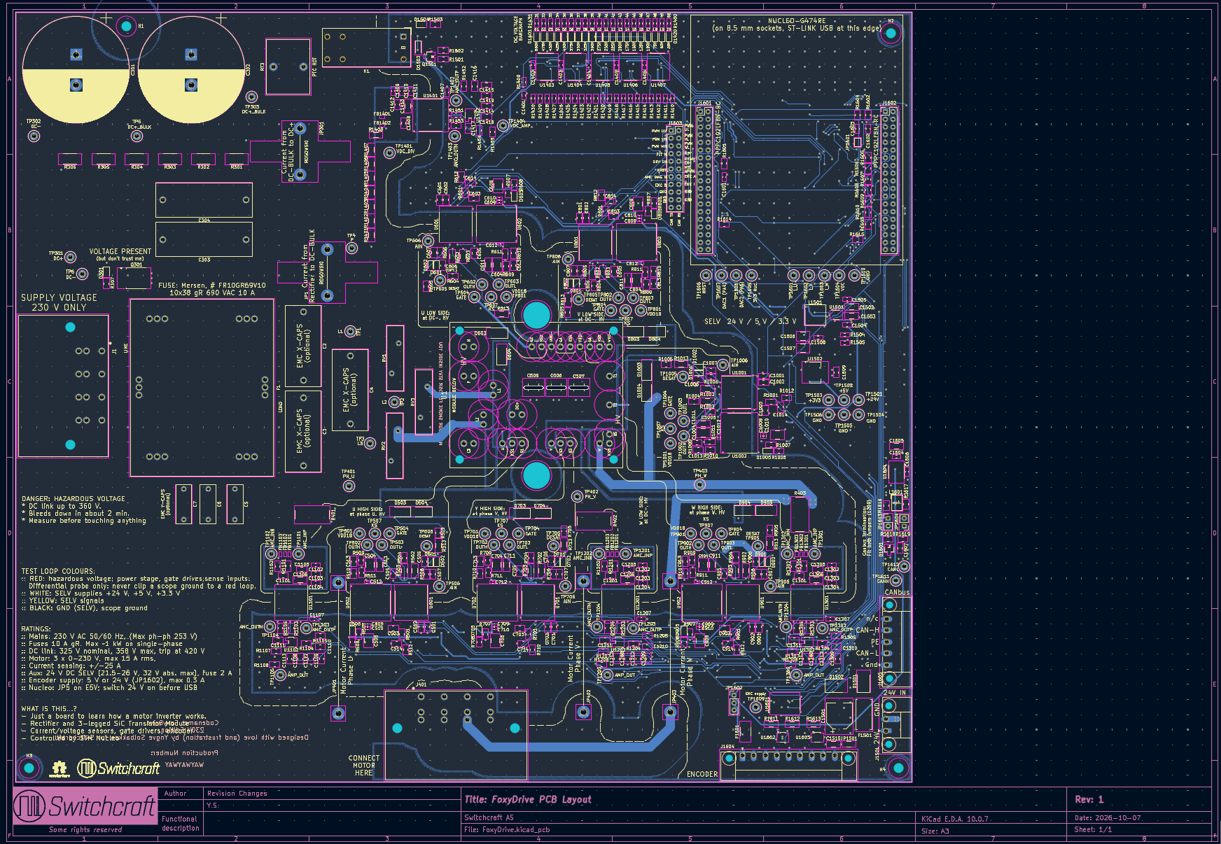
4 layers, 2 oz copper, 296 × 254 mm, designed in KiCad.
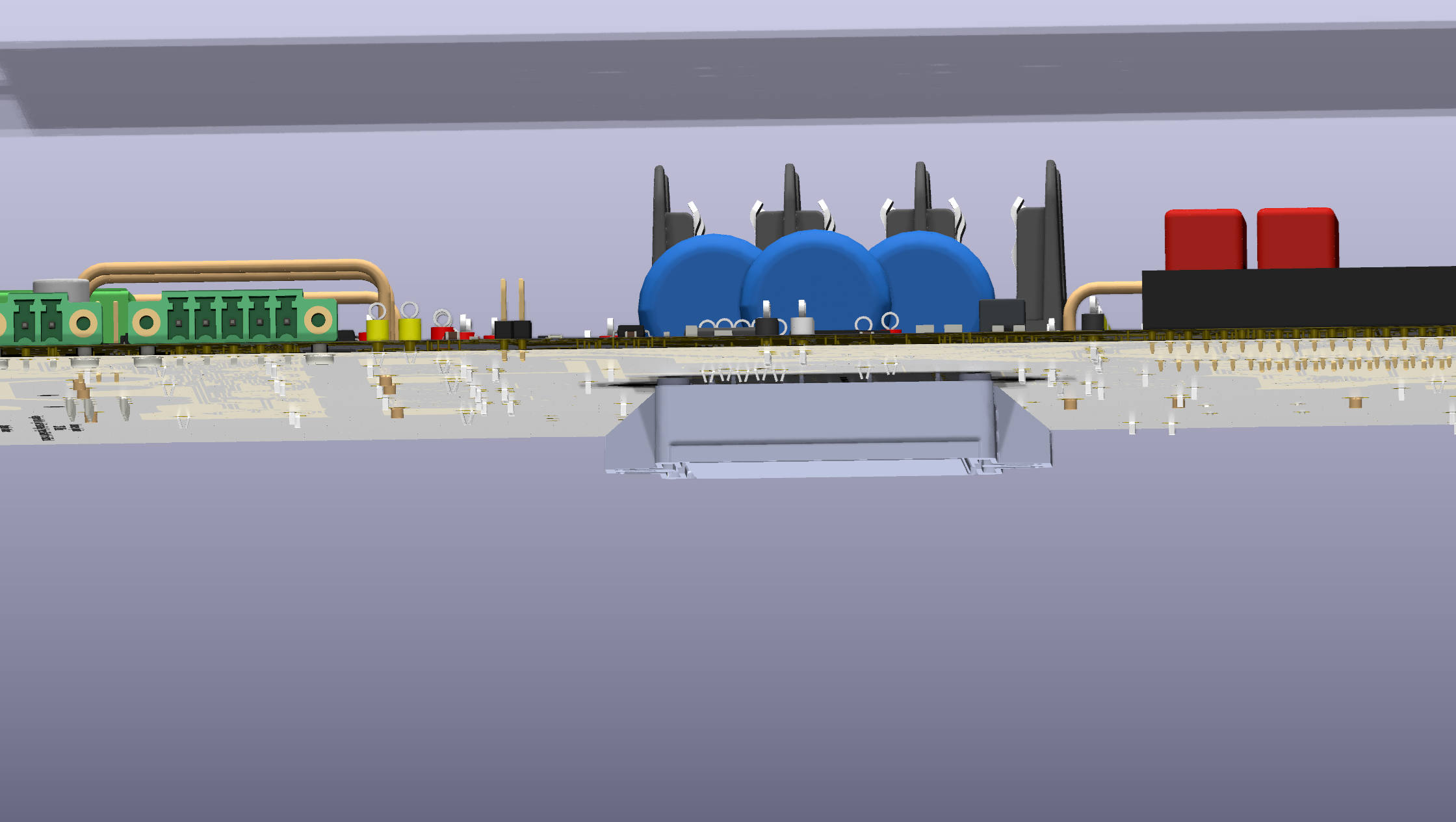
The power module sits under the PCB, and the board stands on a 10 mm aluminium plate which doubles as heatsink for the module.
Fabricated and assembled by a PCB prototyping company
Stats:
568 parts fitted in total, divided into 455 surface mounted parts (SMD) and 113 through-hole (THT)
91 test points (!)
191 resistors
172 capacitors
56 diodes (including LEDs)
32 ICs
9 optional footprints for later part installation (EMC capacitors etc)
17 meter of copper tracks
4839 different track segments
1124 vias
1745 pads
364 nets
40 copper zones
Everything on a board just under A4 format in size
My test motor
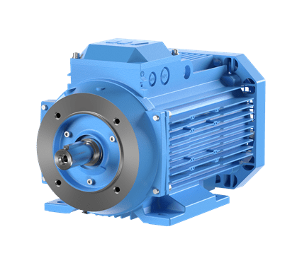
ABB M3AA 80A 4:
0.55 kW, 4-pole induction motor, 1406 rpm, connected in delta on 230 V.
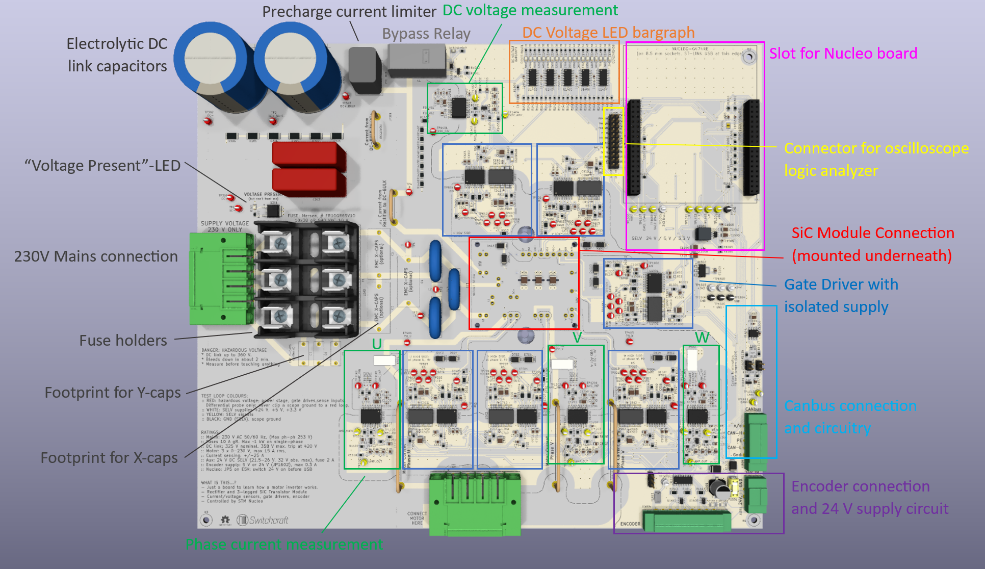
Board overview
Current Status:
Schematic is complete. The layout is placed and routed with a clean DRC, and fab files are generated.
The board is being reviewed and quoted by manufacturer as I am typing this.
Firmware is being developed alongside, on the same G474 Nucleo.
Price: Assume around 5-600 USD for the bare board and around 1000 USD for components and their assembly. If you are going to assemble the board yourself I am guessing you can get the components for about 400-600 dollars.
In a coming article I will share and describe the circuits and their functionality and intent in more detail.
I will also share full drawings and parts list when the board has been tested. I don’t want any of you to order a copy unless I am (at least somewhat) certain that it actually work :)