
When transistors are used to switch large current (as is often the case in power electronics) we face the challenge of how to efficiently control the transistors. The circuits involved in this control are collectively named the gate driver.
The primary purpose of the gate driver is to amplify the current supplied to the gate of the transistor under control. This is required to obtain the fast switching times typically found in switching power electronic converters.
Apart from current amplification, additional features required by the application are often integrated in the gate driver. These include:
- Galvanic isolation of the control signal (and any additional signals)
- Galvanic isolation of the power supply that is responsible for powering the gate driver
- Short-circuit protection of the transistor (Vce desaturation detection)
- Interlock delay time for complementary transistors
Gate driver output amplifier

Simplified schematic of a typical gate driver output stage
The figure at the right depicts the basic principle of a gate driver. The two N, and P-channel MOSFET's are responsible for amplifying the control signal that enters through Rin. Either a positive or a negative voltage is applied to the gate with respect to the emitter, allowing fast turn on, and turn off.
The gate resistor is split in two \(R_{G,on}\) and \(R_{G,off}\). This serves two purposes. First the resistors will limit the shoot-through that will occur at the transition of the conduction states of the output MOSFET's.
Secondly the resistors are used to provide a more fine control of the turn on, and turn of characteristics of the main transistor. More on this later.
The capacitors serve as buffers for the gate driver power supply, delivering the peak currents during switching.
Additionally a resistor of about \(10\;k\Omega - 100\;k\Omega\) should be added between gate and emitter to prevent any unintended charging of the gate capacitor. I.e. to prevent unintended turn on of the transistor.
Gate drive requirements
The purpose of the gate driver is to charge the gate capacitance, also known as the input capacitance. Ideally this should happen as quickly as possible, but limitations of both the gate driver and the transistor imposes restrictions to how fast it may happen.
The gate capacitance is typically stated in the datasheet of the transistor in question. As a example a specific SiC MOSFET (the SKiiP 13ACM12V18) has a specified gate charge \(Q_G = 110nC\), measured at \(V_{GS} = 18V\). This gives us a capacitance \(C_G \approxeq 6nF\)
The power required by the gate driver depends on the switching frequency, and on the energy required at each charge/discharge cycle.
\[ P_{GD} = E \cdot f_{sw} \]
Current is charge per unit time, hence the average required gate current is given by:
\[ I_{G} = Q_G \cdot f_{sw} \]
From this it follows that the power requirements of the gate driver are given by:
\[ P_{GD} = Q_G \cdot (V_{Gon} - V_{Goff}) \cdot f_{sw} \]
The peak gate current is limited by the internal and external gate resistance, as well as any stray inductance that is present in the circuit. It may be approximated by:
\[ I_{G-peak} = \frac{V_{G,on} - V_{G,off}}{R_G + R_{G,int}} \]
The gate driver output typically employs capacitors that are dimensioned to deliver the required gate charge, as this will mitigate the issue of the commonly high internal impedance of the gate drive power supply.
Gate protection

Overvoltage protection by clamping the gate to the supply with a Schottky diode.
In order to protect the gate of the transistor from overvoltage, voltage limitation circuits are often applied. One possibility is to apply zener-diodes (or TVS diodes) between gate and emitter (source).
Another possibility is to use fast switching Schottky diodes to clamp the gate to the driver supply voltage. This possibility is illustrated in the figure at the right.
Gate resistance
The external gate resistance is used to deliberately limit the maximum charge current to the gate. This has several purposes. One is to limit the charge current of the gate, and one is to limit the \(\frac{\mathrm{d}V}{\mathrm{d}t}\) across collector-emitter. Minimum values are often stated in the datasheet of the transistor in question.
In some cases the gate resistance is divided into two resistances, for charge, and discharge respectively. This provides better control over the turn on, and turn off times.
The minimum required gate resistance may simply be calculated by:
\begin{equation}
R_G = \frac{V_{G,on} - V_{G,off}}{I_{G,max}}
\label{eq:gate-resistance}
\end{equation}
Where \(I_{G,max}\) is the maximum permissible gate charge current. This does not necessarily provide the optimum value however.
It is sometimes required to limit the switching times, and thus the charge current of the transistors. The issue is that parasitic inductance in the circuit causes high voltage transients when the currents are switched to quickly.
\[ v = L_s \frac{\mathrm{d}i}{\mathrm{d}t} \]
The gate resistor should thus be optimized for the highest possible rise and fall times, without introducing profound voltage spikes. This will allow for the lowest switching losses. Determining the optimum values analytically can be challenging however, and developers often have to resort to experimentation.
In the case of large transistors and high switching frequency, it is also necessary to compute the power losses in the gate resistor.
\[ P_{R,on} = I_{G,on,RMS}^2 \cdot R_{G,on} \]
Where the RMS value of the gate charge current may be approximated by:
\[ I_{G,on,RMS} = I_{G,on,peak} \cdot \sqrt{\frac{t_{p,on} \cdot f_{sw}}{3}} \]
Similar calculations are performed for the turn off power dissipation. Substituting for the values in the turn of circuit, if they differ.
Over current detection
As the current through the transistor is rising, so is the voltage drop across it (from drain to source, or collector to emitter). The voltage drop is not linear enough to be used in current measurements, but may be used as a indication of a over-current condition. This is typically referred to as \(V_{ce,desat}\) sensing, i.e. collector emitter desaturation voltage sensing in IGBT applications. Desaturation because a saturated transistor would exhibit a low voltage drop.
A voltage threshold is configured, at which the gate-driver over current sub-system is activated. The functionality of this system may be to disable the gate driver, and supplying turn-off voltage to the gate. Additionally a alarm signal is typically fed back to the controller, to allow it to take the appropriate actions.
Because the voltage drop across the transistor will be high in off state, and during switch on, the \(V_{ce,desat}\) monitoring must be enabled and disabled along with the transistor. A short time delay must be added on the enable signal to account for the time it takes the transistor to turn on. This time period is known as the blanking time of the monitoring system. As a interesting side note it seems this blanking time (or at least the nomenclature) is often confused for the dead-time introduced between switching of the transistors.
Signal isolation
In order to safely connect the gate driver to the controller, galvanic isolation is required. The gate driver is floating on a high voltage potential. This isolation is usually achieved through optical or magnetic isolation.
A optoisolator works by optically connecting a light source to a light sensitive device. A typical example is a LED and a phototransistor. When the LED is lit, the phototransistor starts conducting. The optical interface is electrically insulating, able to withstand high voltage differentials. Depending on the required voltage rejection, optical conductors (Optical fiber cable) may be used to increase the distance between sender and receiver.
Typically optocouplers are used to isolate digital signals, although analog signals are also used in some cases.
Optocoupler design considerations
When integrated gate drive circuits are employed, optical isolation is usually included in the package. The reader should refer to the datasheet of the device for how to properly drive the control (LED) input. This section is mostly relevant for those of you who wish to design your own gate driver.
Designing a optocoupler-interface is not particularly difficult, but it is important to consider the parameters of the optocoupler in question.
The input to the LED typically requires a current limiting resistor of appropriate size, depending on the supply voltage. Usually the maximum reverse voltage (PIV) of the LED in an integrated opto-isolator is low, and thus a reverse biased diode is connected in anti-paralell to protect the device in case of reverse connected over voltage. On the transistor side a pull-up resistor is used to keep the collector voltage at logic high, when the LED is off.
It is important to select a optocoupler that is suitable for the application. As a example the 4N25 is a common low performance optocoupler. It is suitable as long as the frequency of the isolated signal remains low. I.e. it might be suitable for a gate driver, but not for a high speed bus signal (e.g. USB).
The current transfer ratio (CTR) of the opto-isolator describes how much of the forward current in the LED is optically transferred to the transistor. E.g. if the CTR is 20% and the LED current is 20mA, this gives us 4mA of collector current. This does not mean that the collector current will be 4mA, as this depends on the biasing conditions. It only means that the maximum is 4mA.
The forward voltage of the LED is used to compute a suitable limiting resistor. As a example for the 4N25, the forward voltage has a typical value of 1.3V. Assuming a logic level of 5V. If a forward current of 50mA is desired(the absolute maximum is 60mA), the resistor is calculated as:
\[ R = \frac{5-1.3}{50\cdot10^{-3}} = 74\Omega \]
The required pull-up resistor on the transistor depends on the loading imposed by the following stages in the circuit, as well as on the signal frequency. Suppose the collector is connected to the input of a microcontroller (advanced gate drivers may have their own microcontrollers) with input capacitance of 7pF. This capacitor must be charged, and the charge time is given by the time constant:
\[ \tau = R \cdot C \]
If we use a 10k pull-up, the time constant is \(70ns\). It is common to assume a charge time of five times the time constant, i.e. \(0.35 \mu s\). The rise and fall times of the 4N25 are specified as typically \(2\mu s\).
The CTR has a typical value of 50%, which gives us 25mA of maximum collector current. The resistor current is given by:
\[ I = \frac{5}{10\cdot10^3} = 0.5mA \]
Which leaves 24.5mA to discharge the input capacitor of the microcontroller, while the charging is limited to 0.5mA. Due to the slow response of the transistor, it is possible (likely) that the input capacitor is discharged before the transistor is fully on however. I.e. the optocoupler is the bandwidth limiting device in this application.
Hopefully the above example illustrates clearly that one should not simply select a opto-isolator randomly.
Power supply isolation
The transistors typically require a voltage of 15-20V at the gate with respect to the emitter. As the emitter may be lifted above ground by hundreds of volts, the various gate drive power supplies must be isolated.
DC-DC converter
A DC-DC converter employing transformers (or coupled inductors in flyback converters) is a popular means of isolation. Integrated converter chips are available, that may be soldered directly to a circuit board.
As transformers only operate on alternating current, a chopper is used to generate a alternating voltage feeding the primary winding. The chopper operates at a high (>100kHz) frequency, in order to reduce the size of the transformer. At the secondary the voltage is rectified and filtered before being supplied to the rest of the gate driver circuity.
By varying the turns ratio, and even splitting the windings, all kinds of voltages can be made available at the secondary.
There are many variations to these converters. Some of which will be covered in a future article.
Isolation transformer
A isolation transformer may be connected at the outputs of the gate drivers. This is a simple and reliable solution, but suffers from lower rise and fall times, when compared to the directly connected gate driver. This type of transformer is known as a pulse transformer, and is a popular choice when driving devices with slower switching characteristics (e.g. thyristors).
If a transformer is to be used, it must have a low leakage flux, i.e. low series inductance. Additionally the primary inductance must be high enough to limit the current.
Bootstrapped power supply
A bootstrapped power supply is (in my opinion) a very interesting way of obtaining isolation. It is not really isolation, but a neat trick to enable the system to withstand the high voltage present in the power stage.
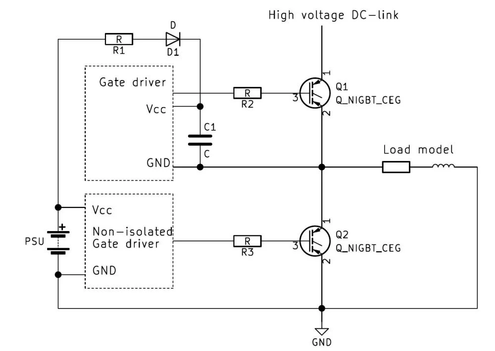
Consider the application of the two-level inverter in the figure to the right. A small capacitor (C1) supplies the gate driver of the high side switch. The anode of a diode (D1) is connected to the low voltage power supply (PSU) and the cathode to the capacitor. The other end of the capacitor is connected to the emitter (or source) of the high side switch.
When the low side switch is conducting, the capacitor is charged through the diode. When the low side switch closes, and the high side switch is conducting, there will be a high voltage at the low end of the capacitor. This reverse biases the diode, and thus the low voltage power supply is protected.
It should be noted that this solution has poor performance, especially if the switching frequency and duty cycles are changing. The only real advantage is low component count (i.e. cheap).
More details are available in this application note.