
While we’re waiting for FedEx, let me introduce you to the functions of FoxyDrive
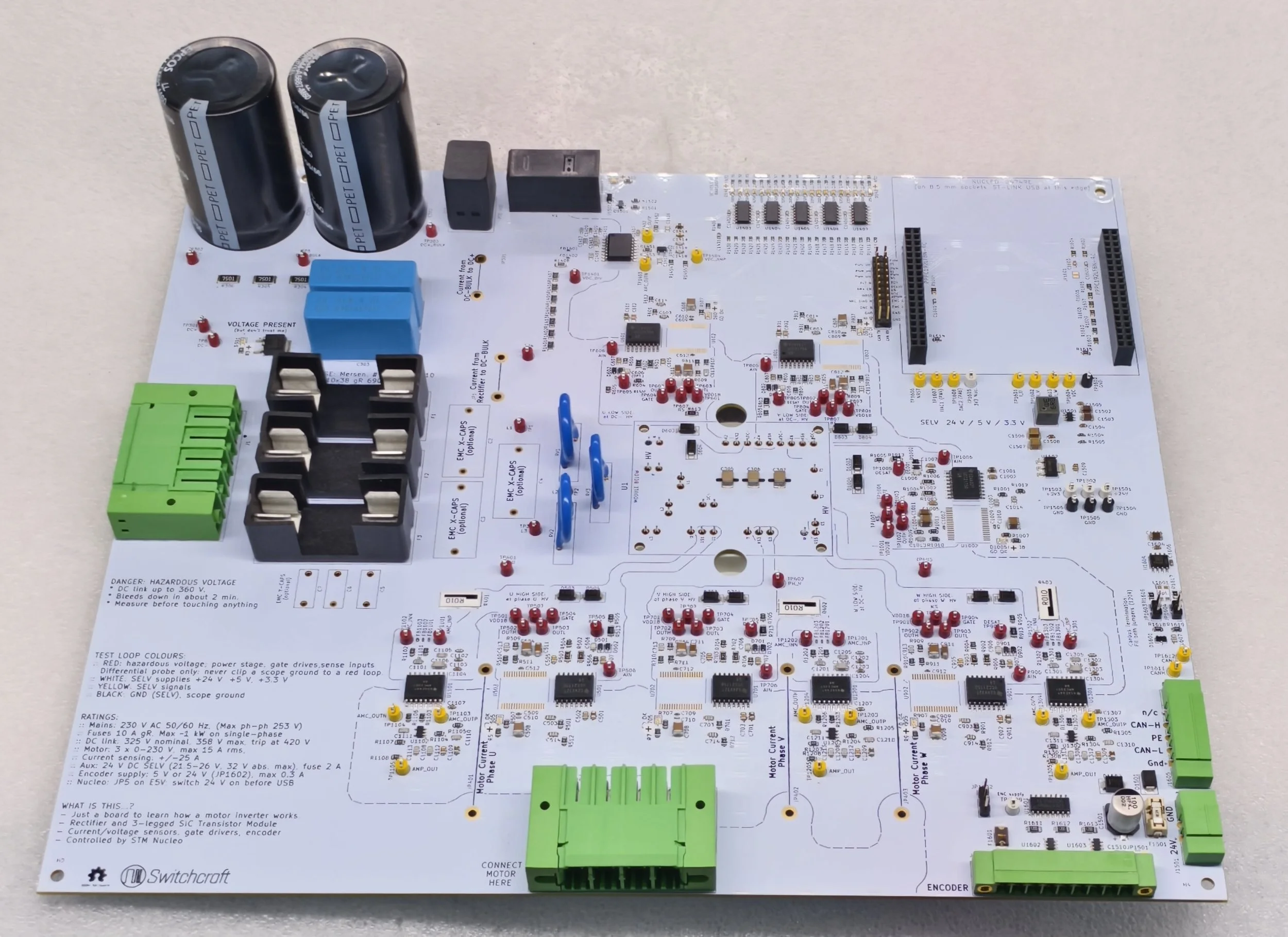
In my previous post about the invertercard, only the design and main specifications was presented.
The current status is that the card is produced, assembled and en route to Norway. The above picture was taken by the QA department before packing it.
While waiting to get my hands on it, I will write up the complete functional description of the card.
The name FoxyDrive was invented on the spot, as I was recently exposed for a beautiful looking Fox on a TV-commercial. Simple as that.
Overview
FoxyDrive V1 is a three-phase motor drive, designed for a small induction motor of around 1 kW. It takes 230 V single-phase mains as input, converts it into about 325 V DC, and uses six silicon-carbide (SiC) transistors, switching about 10-20 000 times per second. It will then syntesize three sine-shaped voltages whose frequency and amplitude is controlled by the software on the controller.
A Nucleo-G474RE microcontroller board is designed to be plugged onto the circuit board and does all the control. Everything the microcontroller can touch is SELV (safety extra-low voltage); it is separated from the mains-connected power circuit by reinforced isolation.
The board is designed to be a learning and experimenting platform:
every single node I found interesting can be reached with a probe,
the gate resistors are easy to change,
wire bridges let a Rogowski current probe measure currents that are normally hidden in copper traces.
Block Diagram
Block diagram showing the power path, the control and gate driver
Main Ratings
Supply: 230V single- or three-phase. Max 253 V between lines.
DC-Link: 325 V nominal, 358 V at 110% mains. Over-voltage trip at 420 V. Capacitors rated to 450 V.
Output: 3× 0-230V, 0- xxx Hz (freq. freely set by firmware, limited by what the motor mechanically can do before bearings etc start to complain. If load is non-moving (resistor or coil), then kHz-range fundamental freq is perfectly doable. Will test later.
Motor: ABB M3AA 80A 4, 0.55 kW, Δ 230 V, 2.24 A, 50 Hz
Power stage capability: ~15 A rms (module 29 A at 70 °C heatsink)
Single phase input limit: ~1 kW (10 A input fuses); DC link sized for 1.5 kW
Switching freq: 10-20 kHz
Control Supply: 24 V DC (keep within 21-26)
Power Path Description: From Input plug to output plug
Input Stage
Purpose: Provide a clean entry, protect against faults, over voltages and EMC + rectify to DC when done.
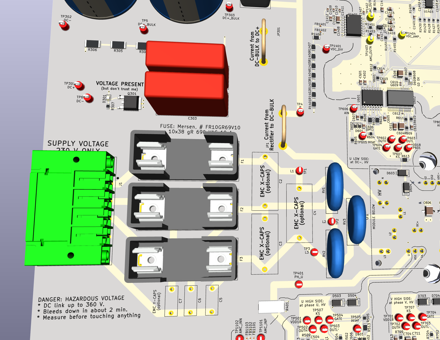
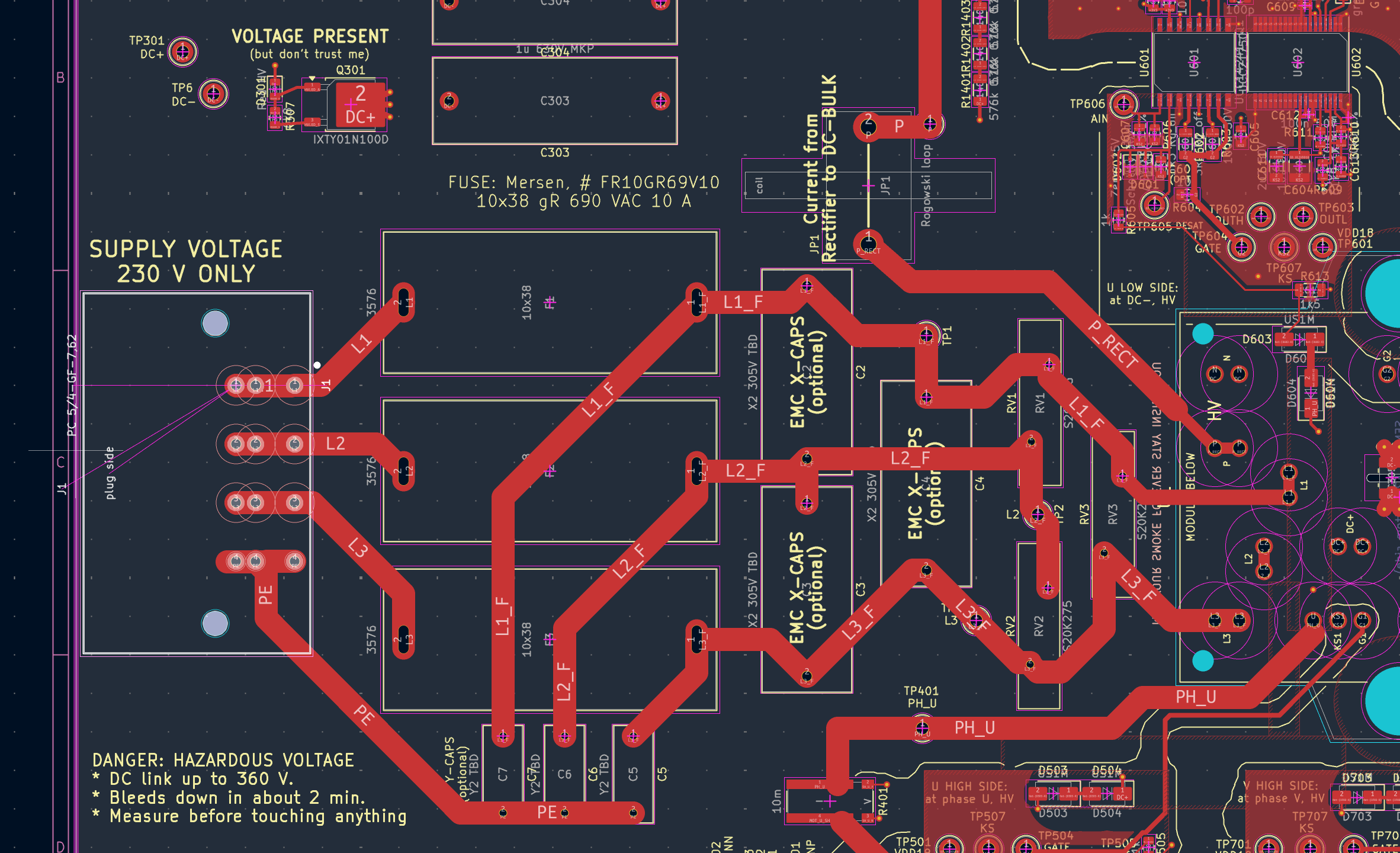
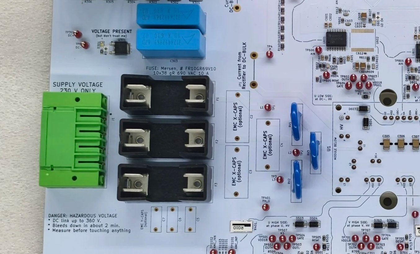
The Input Stage: terminals, fuses, (EMC-filter), surge protection, rectifier, pre-charge
Components with red cross on them are “Do Not Place” (DNP)-components. I will add them later, but will also use the board without them for testing.
Mains input (J1)
The mains arrives through a pluggable, screw-locked connector, J1.
V1 runs on 230 V single-phase or three-phase supply with 230 V between the phases works too, with a fuse link fitted in F3; the limit is 253 V between any two lines. The varistors behind it are 275 V
types, and higher voltage between two lines would destroy them and blow the fuses.PE is connected to the heatsink plate by its own ring lug (M4 hole in the plate's left edge, below J1), not
through PCB copper.The silkscreen next to J1 says SUPPLY VOLTAGE 230 V ONLY: the varistors behind it are 275 V
types, and 400 V between two lines would destroy them and blow the fuses.
Fuses (F1–F3)
Right after the connector, each line goes through a fuse link.
The links are type gR (full-range semiconductor protection): fast enough to protect the rectifier diodes in a short circuit, yet able to carry the normal current continuously.
The important numbers are the I²t values (the "let-through energy" of a current pulse):
the inrush through the precharge PTC is ≈ 3 A²s, about half the 10 A link's melting (pre-arcing) value of 6.7 A²s, so switching on does not blow the fuses,
a short circuit is cleared with at most 55 A²s (at 690 V; less at 230 V), far below what the rectifier diodes survive (365 A²s hot, 685 A²s at 25 °C), so the fuses protect the module.
Placing the fuses first means that a failed (shorted) varistor or rectifier diode is also disconnected.
Surge protection and EMC filter
Three varistors (metal-oxide varistors, MOVs) RV1–RV3 is connected between the lines after the fuses.
A varistor is a ceramic disc that barely conducts below its rated voltage and conducts heavily above it, clamping surges from the mains (lightning, switching of other loads).
The S20K275 type is rated for 275 V rms continuous, just above the highest mains voltage (253 V), and clamps a 100 A surge to 710 V, far below what the module can handle before succumbing.
The capacitors C2–C4 (X capacitors, line to line) and C5–C7 (Y capacitors, line to PE) form an EMC filter. They are footprints only (DNP, do not populate) in V1: the EMC strategy, and especially how much leakage current to PE the Y capacitors may add, is decided later (a 30 mA RCD protects the socket circuit).
Rectifier and JP1
The rectifier is the three-phase diode bridge inside the power module U1 (1600 V, 56 A diodes).
With 230 V on two of its inputs it works as a single-phase bridge.
Its positive output (net P_RECT) goes through the wire bridge JP1, where a Rogowski probe can see the pulsed mains-charging current of the DC link, to net P and the precharge circuit.
The negative output N of the bridge connects straight to DC−.
Precharge (RT3 and K1)
When the mains is switched on, the empty DC-link capacitors look like a short circuit: without a limiter the inrush current would be hundreds of amperes. The precharge circuit limits it:
At switch-on the relay K1 is open, so the current flows through RT3, a PTC thermistor of nominally 100 Ω.
The peak inrush is at most ≈ 13 A (a PTC's resistance is lowest somewhat above room temperature and at high voltage).
Because the bridge only conducts near the mains peaks, charging slows down as the voltage rises: simulated with 100 Ω, the link reaches 90 % after ≈ 1 s and 98 % after ≈ 3 s.
The firmware watches the DC-link voltage. When it has stopped rising (and is above a minimum), it closes K1, which bypasses RT3 for normal operation.
K1 is never opened under load: its contacts cannot break a DC current at this voltage, and opening them would also put the PTC back in series with the inverter current.
The firmware opens K1 only after the inverter has stopped.
A PTC (positive temperature coefficient) resistor was chosen instead of a plain resistor because it protects itself:
if K1 fails to close and the inverter draws current through RT3, the PTC heats up past its reference temperature (130 °C), its resistance rises steeply, and the current drops to a trickle instead of burning the part.
RT3 and K1 sit in parallel between net P and the bulk capacitors (DC+_BULK), so DC− (the reference for the low-side drivers and the DC-link voltage measurement) is never switched.
DC Link
Purpose: Keep supply at steady level, store energy for the swithching.
The DC link is made up from several different capacitors with different properties.
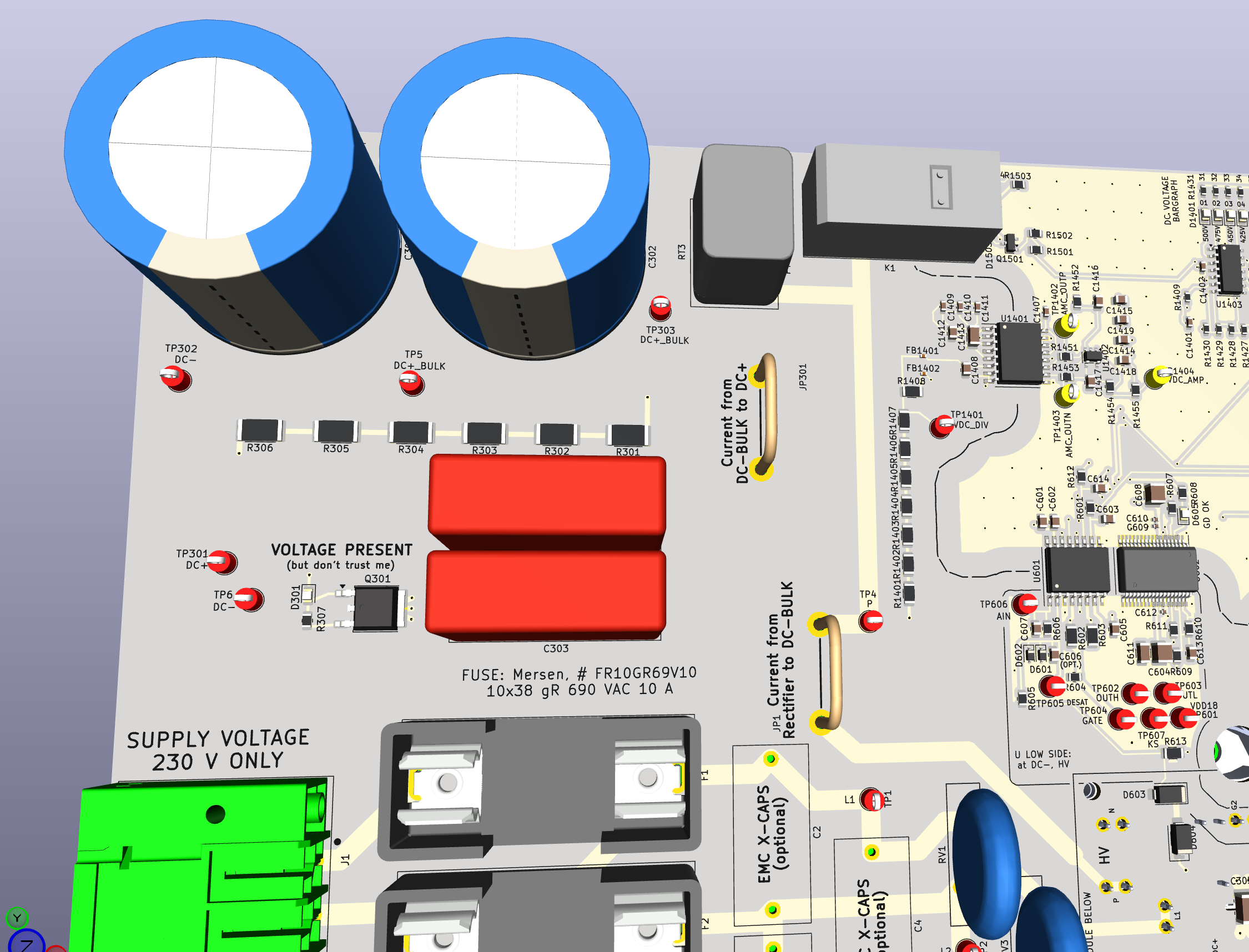
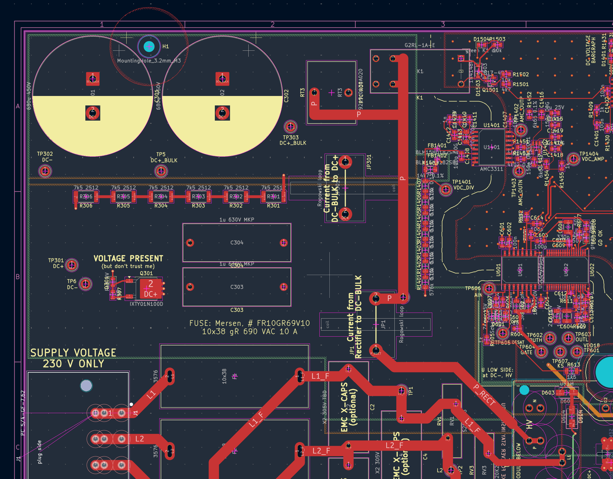
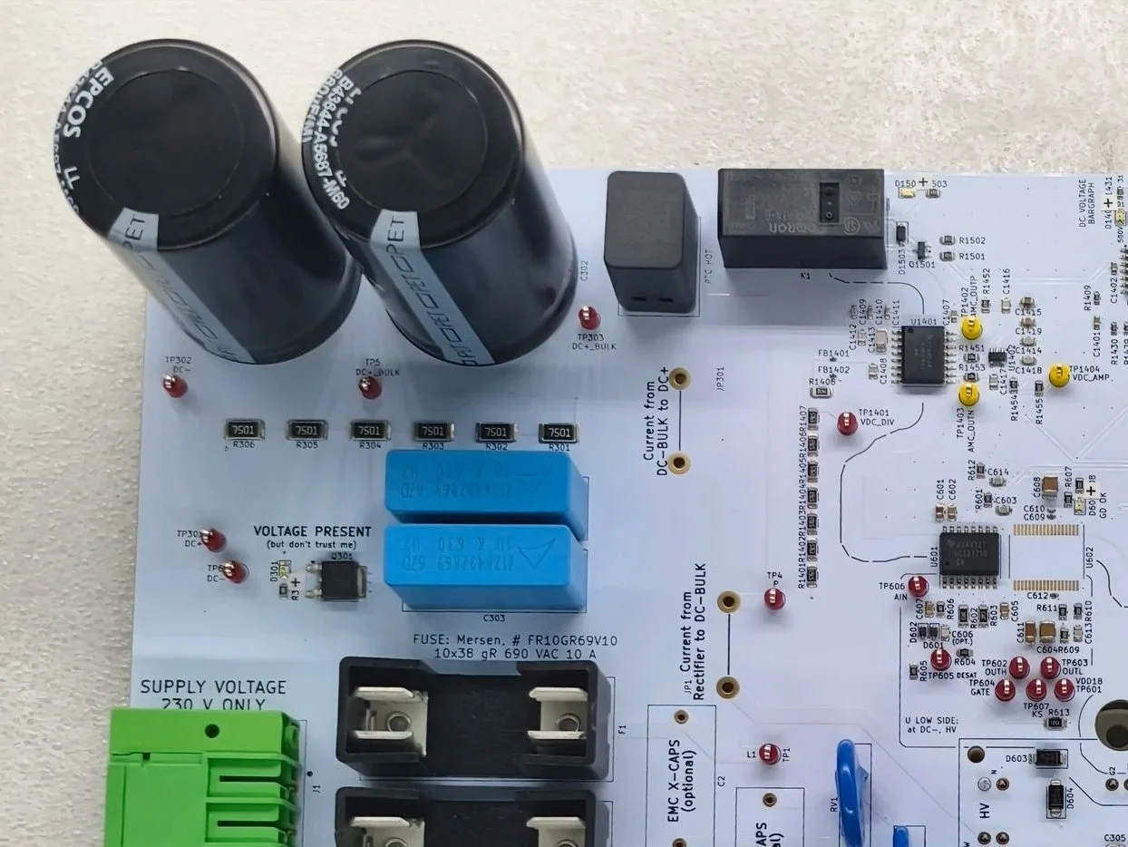
The DC link stores energy between the mains peaks and supplies the inverter's pulsed current. It consists of:
Bulk capacitors C301, C302
(2 × 680 µF, 450 V, snap-in electrolytic, in parallel = 1360 µF).
They carry the 100 Hz ripple: at 1.5 kW the DC-link voltage dips ≈ 27 V between mains peaks.
Electrolytics are the only practical choice for this much capacitance at this voltage.
Bleeder resistors R301–R306
(6 × 7.5 kΩ in series) slowly discharge the link when the mains is removed:
from 358 V to below 60 V in about 109 s (requirement: < 2 min).
They dissipate 2.85 W continuously.
HV-present LED D301,
fed from the DC link itself through a current source (Q301, R307):
it lights as long as there are more than a few volts on the link, even with the 24 V supply off.
It is a reminder, not a safety device: always measure before touching.
Wire bridge JP301
between the bulk bank (net DC+_BULK) and the module side (net DC+):
with a Rogowski probe here you can see how the ripple current splits between the electrolytics and the film capacitors.
Film capacitors C303, C304
(2 × 1 µF, 630 V, polypropylene) sit in the DC-link corner next to the electrolytics,
about 105–120 mm from the module, and reach it through the stacked DC+/DC− planes.
They take the switching-frequency ripple current that the electrolytics, with their internal inductance and resistance, cannot deliver.
Ceramic capacitors C305–C307
(3 × 100 nF, 630 V, 1812) sit right at the module's DC pins.
They supply the fastest part of each switching edge and keep its voltage overshoot small.
Inverter Power Module and Output Stage
Purpose: To switch. Rapidly. Fearlessly. Stupidly.
The SiC inverter and its main outputs toward the motor connector plug.
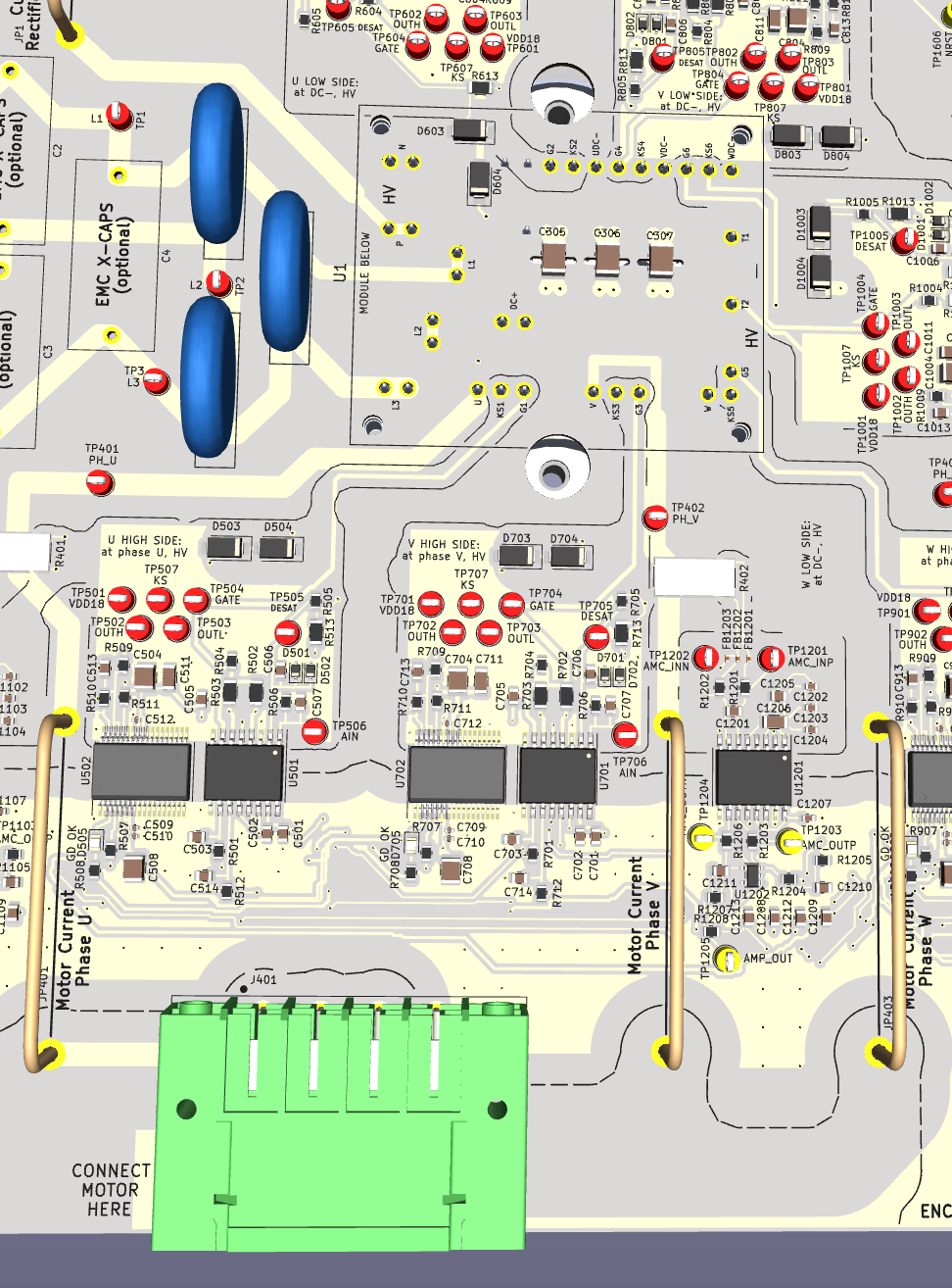
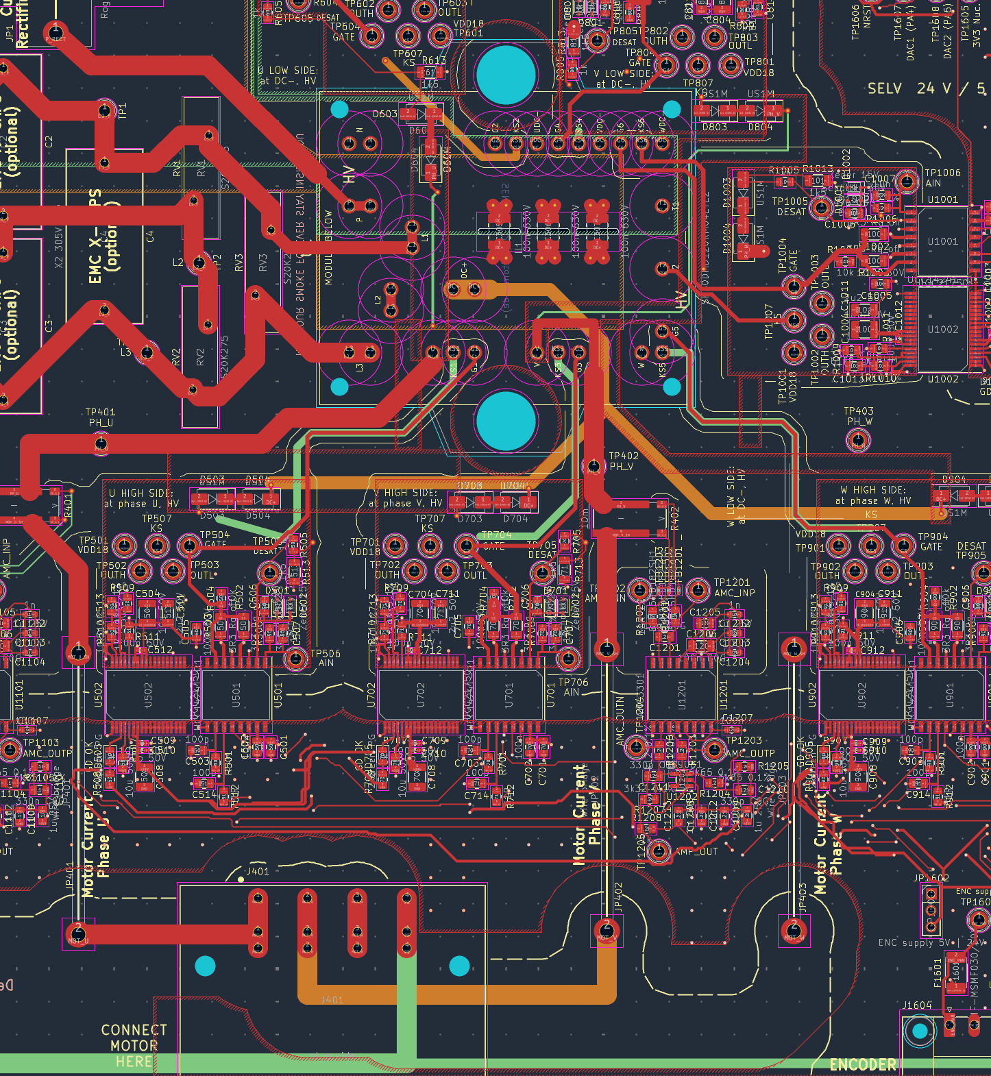
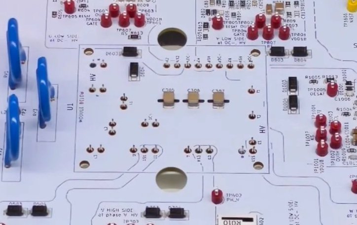
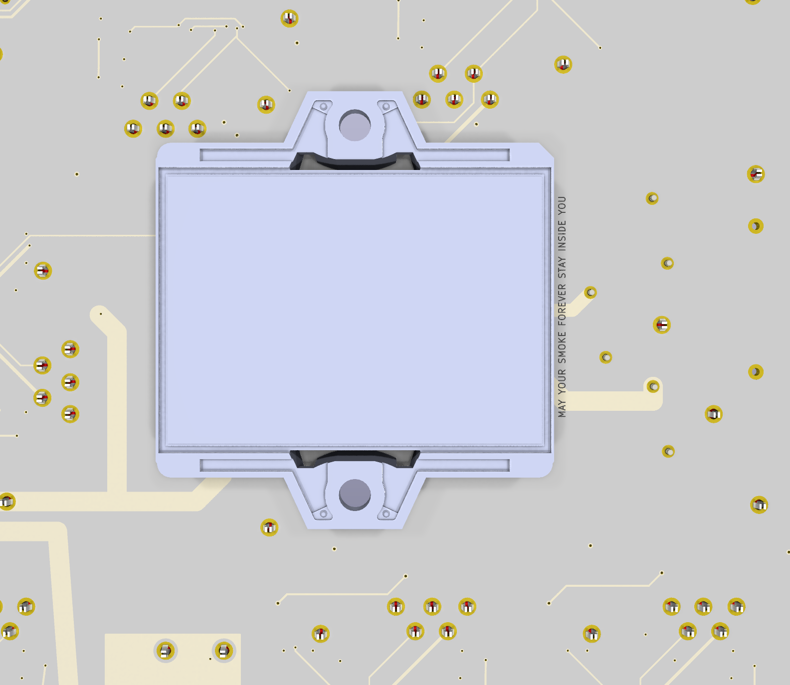
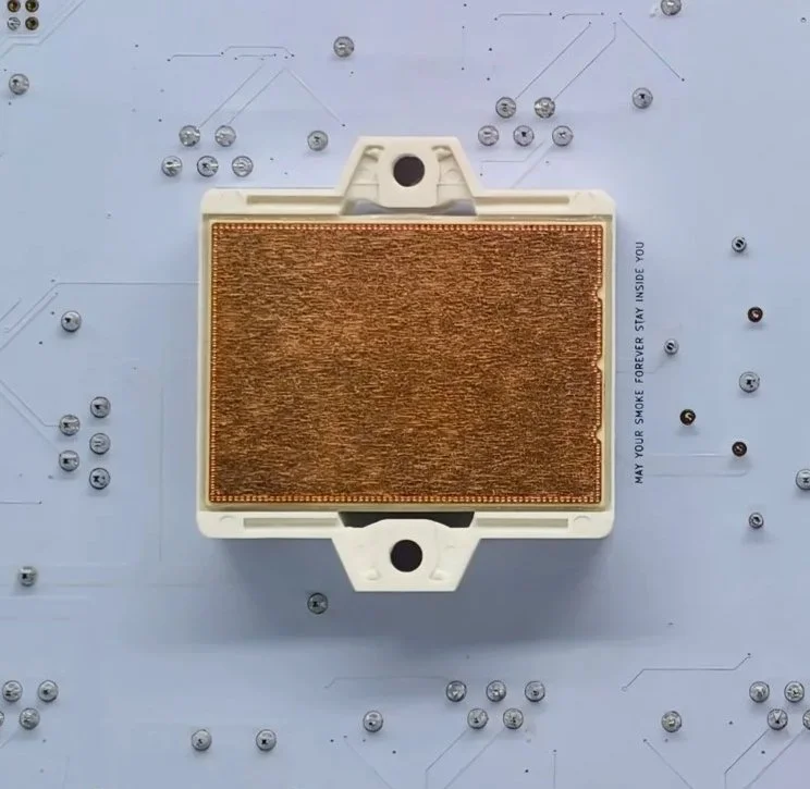
Inverter (power module U1)
The six SiC MOSFETs live in the Semikron SK30DMD120RM04ETE2 module together with the rectifier and a temperature sensor (NTC).
Three legs (U, V, W) each have a high-side and a low-side MOSFET.
Each MOSFET has a gate pin (G1…G6) and, next to it, a source pin that we use only as the gate's return path ("pseudo-Kelvin source", KS1…KS6).
This keeps the large output current out of the gate loop, which would otherwise disturb the gate voltage at every switching edge.
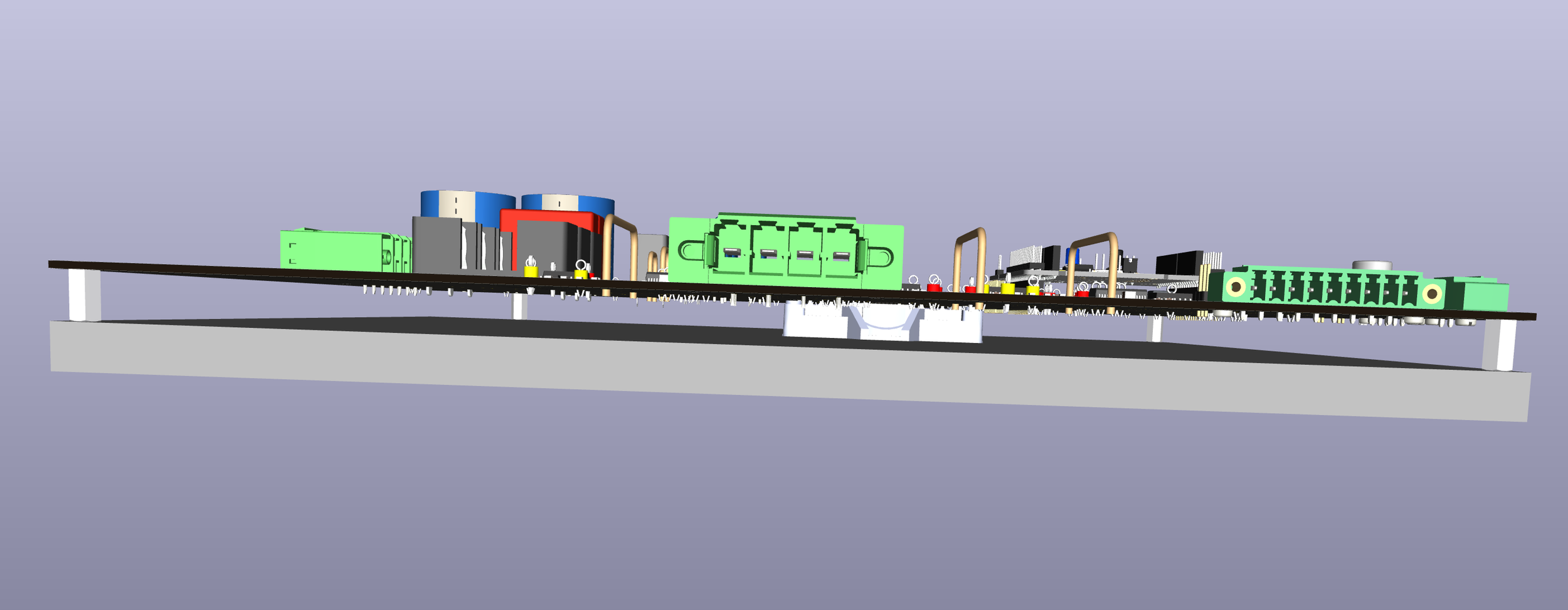
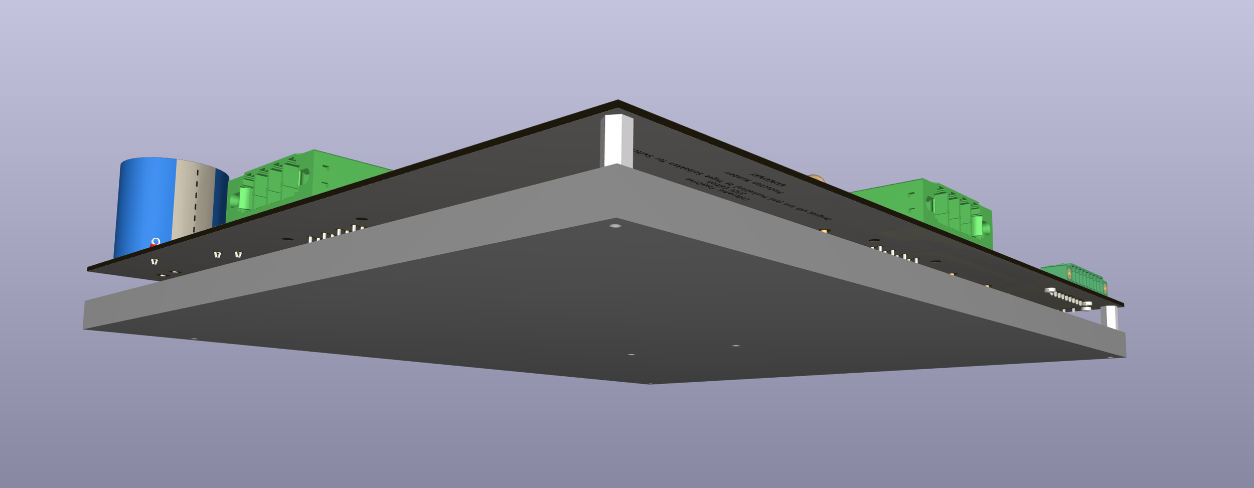
The module is mounted under the PCB, pressed onto the heatsink: a board-size, 10 mm thick black-anodised aluminium plate, on which the PCB stands on four M3 × 12 mm spacers at its corners.
The module's press-fit pins are soldered into the board. Each gate is driven by its own gate-driver cell.
The module's NTC is read by the W low-side driver.
For the present 0.55 kW motor (3.2 A peak), the module is lightly loaded: losses are a few watts in total. At the 15 A rms design capability they would be ~100 W.
Phase outputs, shunts and J401
Each phase output leaves the module through a shunt resistor R401–R403 (10 mΩ, 4-terminal).
The current through the shunt makes a small voltage (10 mV per ampere) that the current-sense cells measure.
After its shunt each phase passes a raised wire bridge JP401–JP403: on the board the motor leads have to cross the strip of SELV copper that joins the input sides of the high-side drivers and current-sense cells to the controller, and they do it in the air, on a 2.5 mm² copper arch.
The same arches give a Rogowski probe access to every phase current.
The motor is connected to J401, the same Phoenix connector type as the mains input (poles U, V, W, PE).
On 230 V the motor is connected in delta (Δ).
Gate Driver Cells
DC-bias supply to the left, gate driver circuit to the right. 3.3 V-signaling in the middle.
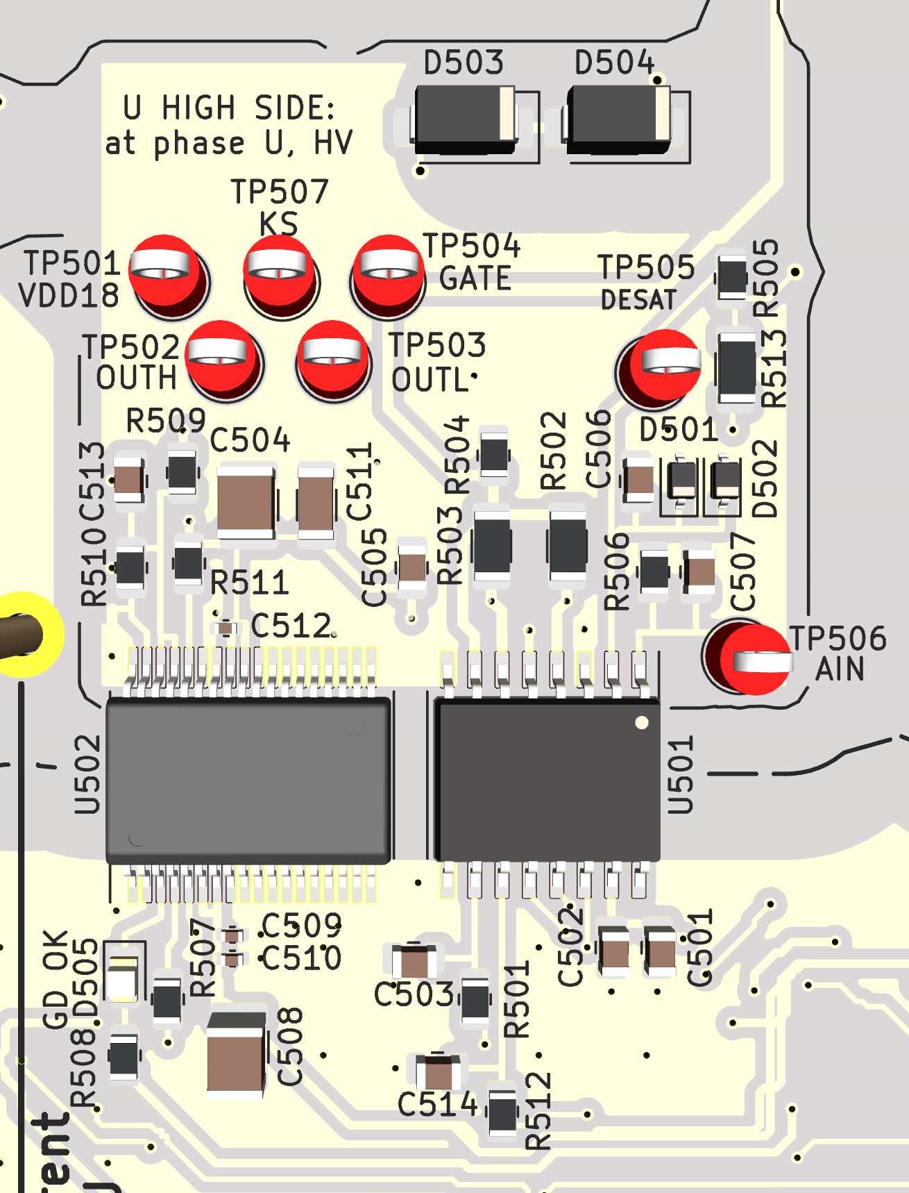
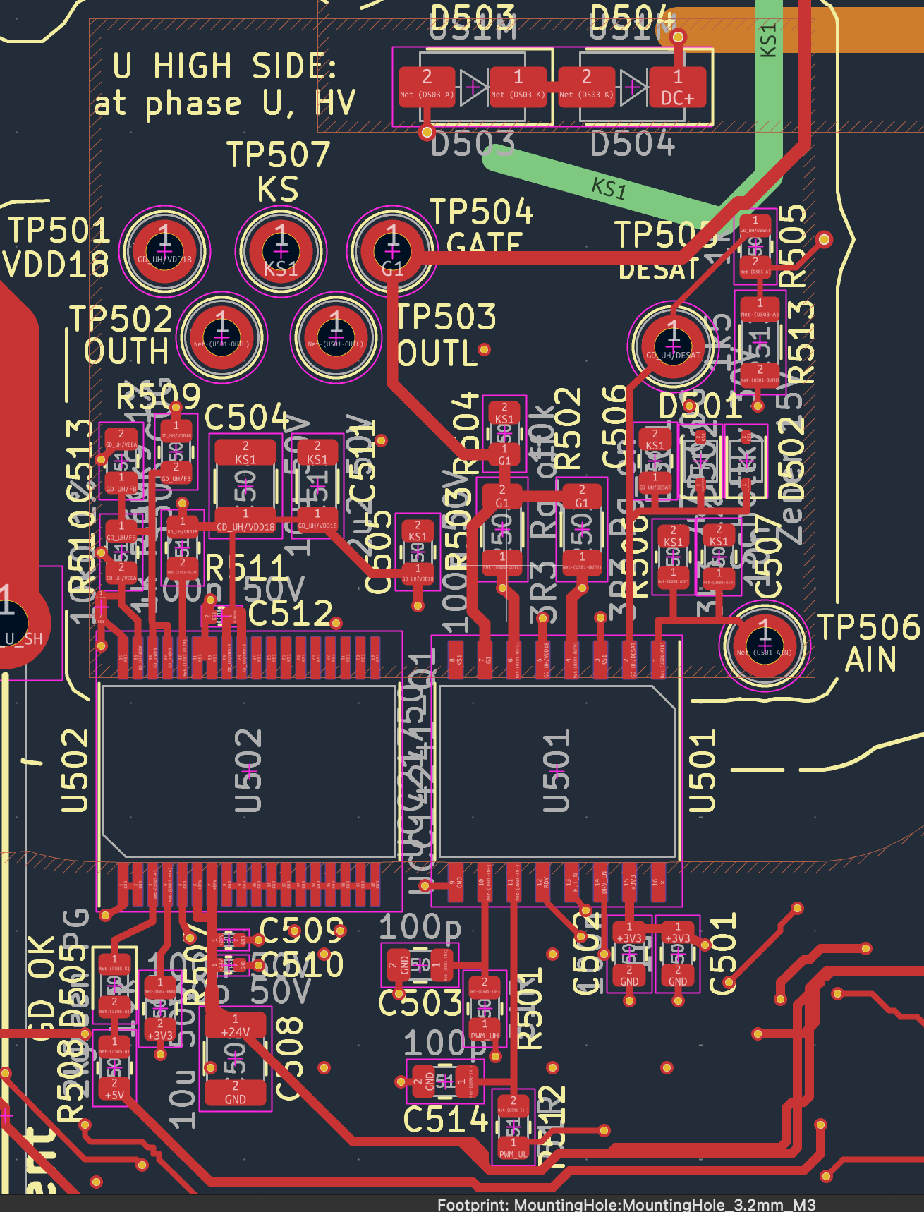
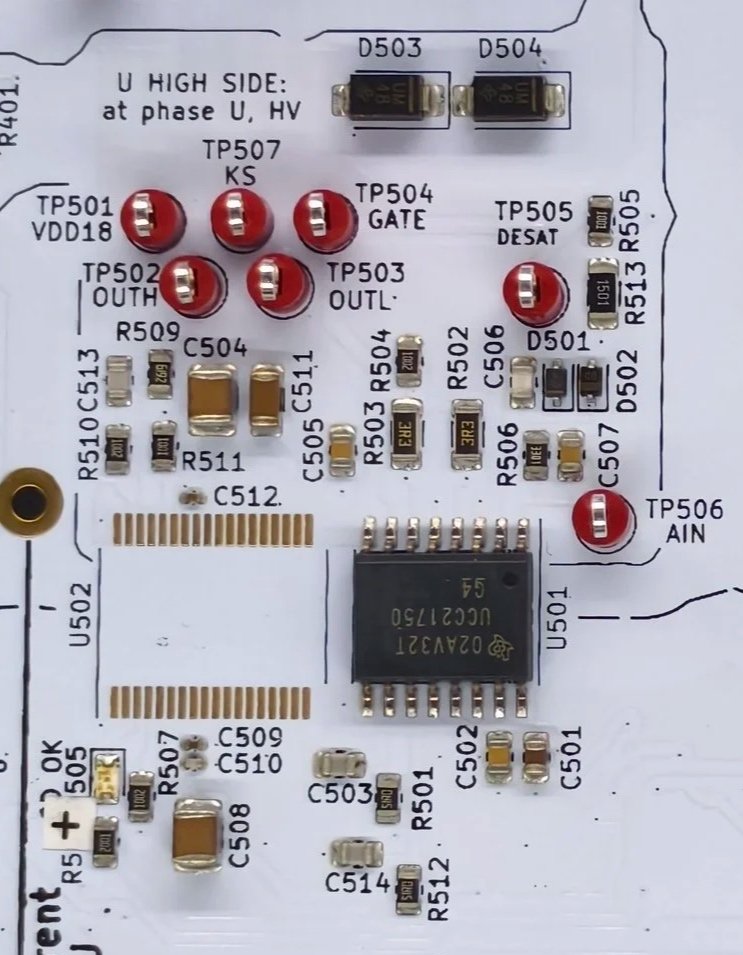
A gate-driver cell takes a 3.3 V PWM signal from the microcontroller and turns the MOSFET on and off with 0 V / 18 V between its gate and source, across an isolation barrier.
It contains:
Isolated bias supply
Parts: U502; TI UCC15241-Q1, and its capacitors and resistors.
Purpose: makes an isolated 18 V supply for the driver's output side from the 24 V SELV supply.
The gate driver's output side floats with the MOSFET's source, so it needs its own supply. U502 is a complete isolated DC/DC converter in one 36-pin package: a transformer and its controller, switching at about 13 MHz.
It takes 24 V on its primary side (pins 1–18, SELV) and delivers an isolated output on its secondary side (pins
19–36, island).
The isolation is reinforced (5000 V rms for 1 minute, 1000 V rms continuous working voltage) and the barrier has less than 3.5 pF of capacitance, so the fast voltage jumps of the floating side push very little
current into the 24 V supply.
Gate driver
Parts: U501; TI UCC21750
Purpose: carries the PWM across the isolation barrier and drives the gate (up to 10 A peak capability).
U501 is a single-channel isolated gate driver.
Its left half (pins 9–16) talks to the microcontroller at 3.3 V; its right half (pins 1–8) drives the gate.
Between them is a capacitive reinforced isolation barrier (5.7 kV rms for 1 minute, 1.5 kV rms working voltage) that tolerates voltage jumps of at least 150 V/ns (CMTI; the module switches at about 30 V/ns).
Gate network
Parts: R502, R503, R504, the CLMPI connection
Purpose: sets the switching speed and holds the gate off
R502 (Rg_on) and R503 (Rg_off), 3.3 Ω each set how fast the gate charges and discharges, and therefore how fast the MOSFET switches (dv/dt, di/dt). 3.3 Ω is the value in the module datasheet's switching tests.
Larger values give slower, gentler edges (less EMC noise, less stress on the motor insulation, more switching loss). They are 1206 parts so they are easy to change by hand: this is one of the planned experiments.
Peak gate current at turn-on ≈ 18 V / (3.3 Ω + 1.0 Ω inside the module + 0.7 Ω inside the driver) ≈ 3.6 A; at
turn-off ≈ 18 V / (3.3 + 1.0 + 0.3) Ω ≈ 3.9 A.
CLMPI (Miller clamp) connects directly to the gate. When the opposite switch turns on, the fast voltage rise
pushes current through the MOSFET's internal gate–drain capacitance (the Miller capacitance) into the gate, which could turn it on by mistake. Once the gate is below 2 V (after a normal turn-off), the clamp shorts it to the source through a switch inside the driver, bypassing Rg_off.
R504 (10 kΩ) gate–source keeps the gate off when the cell has no supply (during power-up, or with a driver
removed). The driver's own pull-down only holds the gate at about 2 V in that state.
Short-circuit detection (DESAT)
Parts: R505, D503, D504, C506, D501, D502.
Purpose: switches the MOSFET off if it is on but its voltage does not collapse.
When a MOSFET is on, the voltage across it is small (current × on-resistance, a few volts at most). In a short circuit the current rises so far that the voltage climbs (the transistor "desaturates"). The driver watches for this:
While the gate is on, an internal 500 µA current source pushes current out of the DESAT pin, through R505 (1 kΩ) and the two high-voltage diodes D503, D504 into the MOSFET's drain.
If the drain voltage is low, the diodes conduct and DESAT stays low. If the drain voltage rises, the diodes block, the current charges the capacitance on the DESAT node, and when DESAT reaches 9.15 V the driver trips. That capacitance is the blanking capacitor C506 (47 pF C0G) plus the two clamp diodes D501/D502, the pin and the copper (≈ 95 pF in total).
How fast is it? The module survives a short circuit for 2 µs (at up to 720 V; we have 358 V):
Leading-edge blanking (the current source starts after it): 0.20 µs
+DESAT node charged to the threshold through R513 + R505 (2.5 kΩ) from OUTH: 0.17 µs
+Deglitch filter and delay to the output: 0.20 µs
+Soft turn-off of 91 nC gate charge: 0.23 µs
=Total time: ≈ 0.8 µs (typical), 1.1–1.3 µs worst case
Analog channel
Parts: R506, C507 (+ module NTC on GateDriver_W-Lower only)
Purpose: sends the module temperature across the barrier
The UCC21750 has a spare isolated analog channel:
the voltage on AIN (0.6–4.5 V, measured against COM) is converted to a 400 kHz PWM signal on APWM, whose duty cycle tells the voltage: D = 100 % − 20 % per volt × V_AIN.
The module's NTC (5 kΩ at 25 °C) has only functional insulation inside the module and sits next to the W low-side switch, so it is read by the W low-side driver:
T1 → R1006 → AIN, T2 → KS6 (that driver's ground).
An internal 200 µA current source in AIN biases the NTC. On its own, the NTC's voltage (200 µA × 5 kΩ = 1.0 V at 25 °C) drops below the 0.6 V lower limit above ~38 °C, exactly the range that matters.
The 3.3 kΩ resistor R506/R1006 in series adds a constant 0.66 V, which keeps the reading in range from about −5 °C upwards.
C507 (10 nF) filters switching noise. In the other five cells the AIN sheet pin is tied to the cell ground on the root sheet, so AIN sits at a harmless 0.66 V and APWM is left unconnected.
Inputs and status
Parts: R501/C503, R512/C514, D505/R508, R507
Purpose: input filters, interlock, bias-OK LED, enable
DC Bias Enable and status.
ENA is pulled to 3.3 V through R507 (10 kΩ): the supply starts as soon as 3.3 V exists.
Removing R507 keeps that one cell switched off (useful in bring-up).
The open-drain PG output lights the green LED D505 when there is no fault and the output is within ±10 % of its target: six green LEDs = six healthy gate supplies.
GateDriver Inputs:
IN+ receives the cell's own PWM through a 51 Ω / 100 pF filter (R501, C503) that removes nanosecond noise spikes without delaying the signal noticeably (τ ≈ 5 ns).
IN− receives the PWM of the other switch in the same leg, through the same filter (R512, C514). The driver
only switches on when IN+ is high and IN− is low, so the two switches of a leg can never be on together, even if the firmware makes a mistake. This is the hardware interlock.RST/EN (from DRV_EN) enables the driver and resets it after a fault. An internal pull-down keeps the driver off until the microcontroller enables it.
FLT (fault) and RDY (supplies OK) are open-drain outputs, wired together across all six drivers;. FLT low will stop all PWM immediately (it goes to the timer's break input).
Test points
Parts: TP501–TP507
Purpose: VDD18, OUTH, OUTL, GATE, DESAT, AIN, KS
Each cell has seven test loops:
VDD18,
OUTH, OUTL (driver outputs before the gate resistors),
GATE (after them),
DESAT, AIN and KS (the cell ground).
GATE and KS are a close pair for the gate-voltage probe.
Gate measurements are best done on a low-side switch: the high-side island jumps 325 V at every edge, which corrupts even a good differential probe at high frequency.
Preventing both switches of a leg closing together
This is the worst distaster the inverter can face: closing both the upper and lower switch creates a short circuit between DC+ and DC-. It must be prevented at all costs.
There are two possible causes and three different ways to protect against it.
First the two causes:
Software, firmware or hardware glitch causes a high signals on two corresponding switches at the same time.
A parasitic signal picked up by the board activates a gate where the other gate is already closed
And the three levels of protection:
Dead time: MCU hardware, set by firmware:
The MCU timer TIM1 generates complementary PWM signals. CH1 and CH1N come from the same compare value, so the firmware never sets the upper and lower switch separately. The timer’s dead-time generator delays every rising edge, so one output always goes low before the other goes high.Register setup in the Nucleo Microcontroller Unit (MCU):
TIM1_CCER: CC1E + CC1NE (and the same for CH2/3) enable the complementary pairs.
TIM1_BDTR.DTG[7:0]: dead time in timer ticks (about 5.9 ns per tick at 170 MHz in the lowest range).
TIM1_BDTR.MOE: master output enable.
Once the timer is set up, a bug in the control loop (a wrong duty, a NaN, an overflow) can’t produce overlap, because the pair is generated in hardware from one number.
The real risks are configuration errors, such as DTG = 0, a wrong polarity bit (CCxP/CCxNP), or driving a pin as plain GPIO instead of its timer function.
We will cover this in much more detail when presenting the MCU register configuration.
Cross-interlock at the driver inputs: board hardware
On the board it’s the IN+/IN− wiring (R501/C503 and R512/C514 in each cell). Each gate driver has an IN+ and an IN- input.
The UCC21750 output goes high only when IN+ = 1 and IN− = 0.
If both PWMs are high, whether from a misconfigured timer, a debugger halt with a wrong idle state, or a pin glitch, both drivers hold their gates low.
No firmware error can get past this, because it’s wired on the board.
The interlock has one limit: it stops overlap at the inputs but adds no dead time. A MOSFET takes time to turn off: propagation delay, skew between the two driver ICs, and gate discharge through Rg_off.
With zero dead time, one switch would start turning on while the other is still turning off, giving a short shoot-through spike on every edge.
Layer 1 is still needed, and this interlock is the safety net under it.
DESAT and the break input: last resort
If both switches still conduct (a failed MOSFET, a gate damaged by a transient, a short in the motor cable), the current rises within a few hundred ns.
The DESAT circuit sees V_DS climb past about 6–7 V, the driver soft-turns-off its switch in about 1 µs, and pulls FLT_N low.
That line goes to PA15 = TIM1_BKIN: the timer clears MOE (master output enable) in hardware and puts all six outputs in their idle state without waiting for software (TIM1_BDTR.BKE, plus OISx/OISxN = 0 in TIM1_CR2).
The comparators on the phase currents trip the same break input for slower overcurrents.
Measurement Circuits
What you can’t see, you can’t control.
What you see incorrectly, you control incorrectly.
Thus, measurements required, accuracy demanded.
Phase Currents (3 identical cells)
Isolated SELV side on the left, HV side measurement circuitry to the right
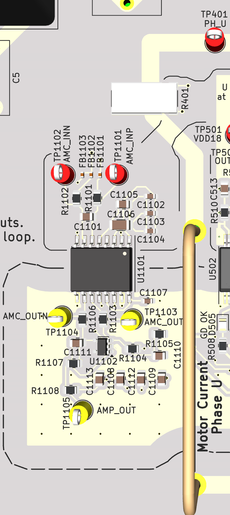
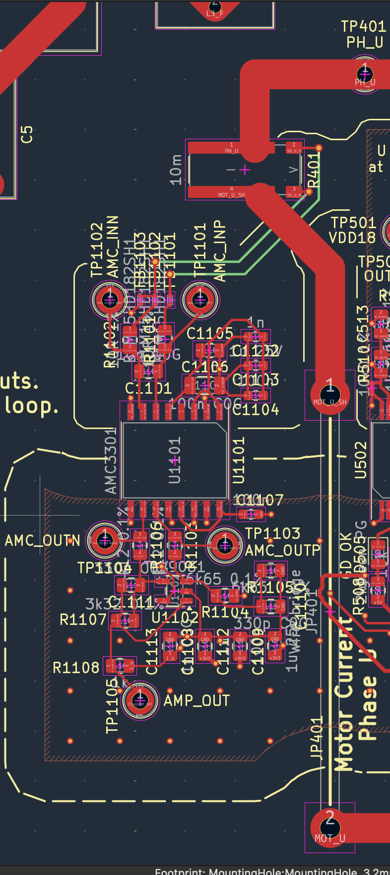
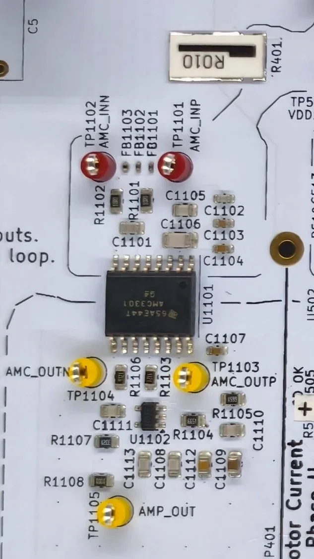
Chain:
shunt R401 (10 mΩ, 10 mV/A)
→ input filter (ferrite beads FB1101/FB1102, 10 Ω R1101/R1102, 10 nF C1101)
→ AMC3301 isolated amplifier U1101 (gain 8.2)
→ difference amplifier U1102 (TLV9061, gain 0.806, centred at 1.65 V)
→ 1 kΩ + 1 nF (R1108, C1113)
→ signal I_U to the microcontroller's 12 bit ADC and comparator.
The ABB motor's peak current (3.2 A) uses about ±260 counts around mid-scale. The resolution is 12 mA.
Hardware overcurrent protection: The same signal also goes to an STM32 comparator whose threshold (a DAC) the firmware sets at ~6–8 A peak: an overcurrent switches the PWM off in hardware, without waiting for software.
The isolated amplifier (AMC3301). Its input side floats with the phase output and is powered by a small isolated DC/DC converter inside the package, so no separate floating supply is needed.
Inside, a delta-sigma modulator samples the input at 20 MHz and sends the bit stream across the reinforced barrier (85 V/ns transient immunity; the module switches at ~30 V/ns); the output side turns it back into a differential voltage (334 kHz bandwidth). The circuit is TI's recommended one (datasheet SBAS917C, Fig. 7-2 and 7-5).
The difference amplifier (U1102, TLV9061). It turns the AMC3301's differential output into one voltage for the ADC, scales ±2.05 V down to ±1.65 V and lifts it to the middle of the ADC range:
V_out = 1.65 V + (3.32 kΩ / 4.12 kΩ) × (OUTP − OUTN) = 1.65 V + 0.806 × (OUTP − OUTN).
Firmware: measure the zero (PWM off) at start-up and subtract it; calibrate the gain once against a known current if better than about 1 % is needed.
Test points (per cell):
AMC_INP/AMC_INN (input side, at phase potential: differential probe only),
AMC_OUTP and AMC_OUTN, AMP_OUT (op-amp output).
The ADC pins have TP1601–TP1603 on the controller sheet.
DC Link Voltage
Main DC link on the left, with resistor divider chain. Measurement and scaling on the right hand side.
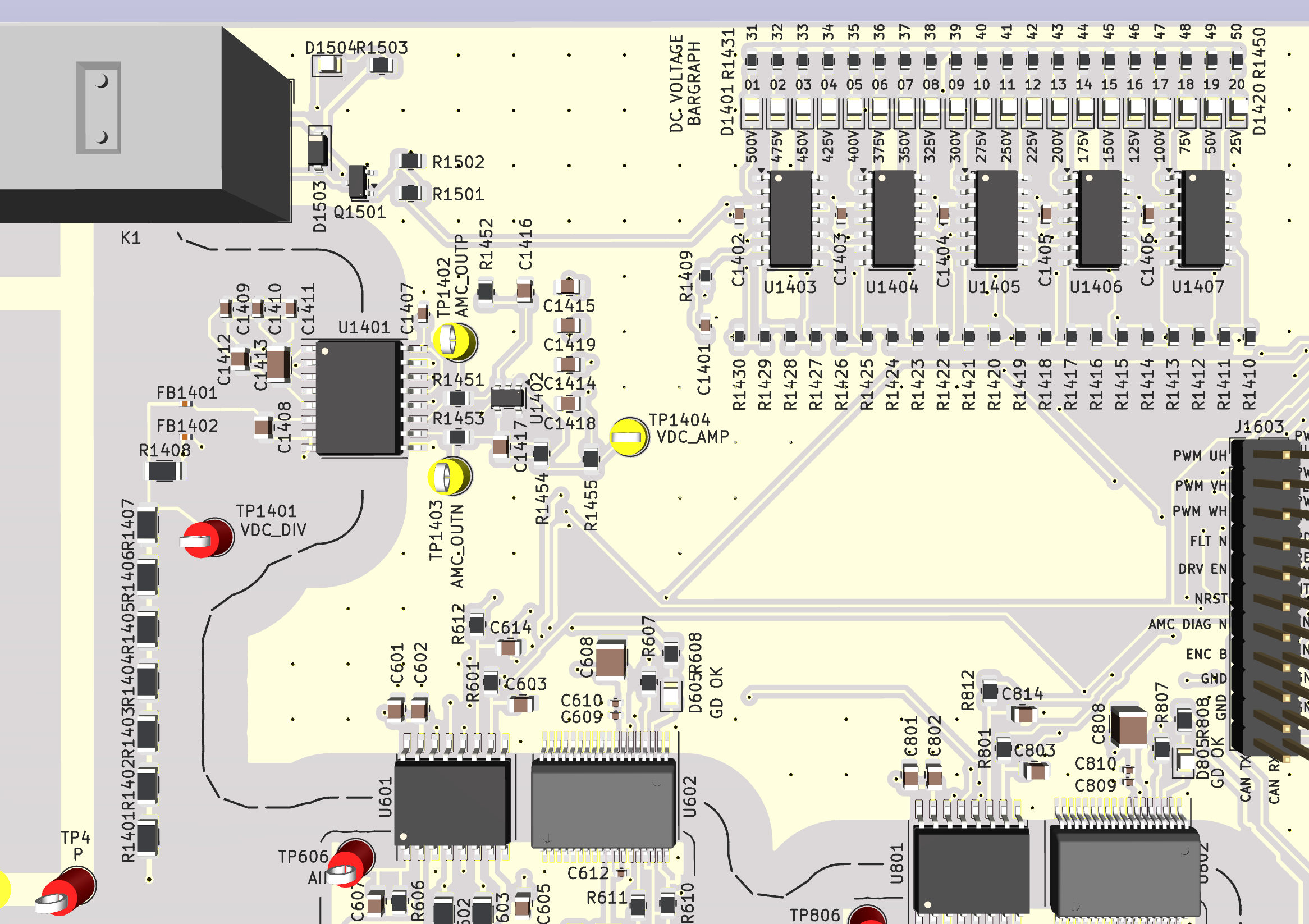
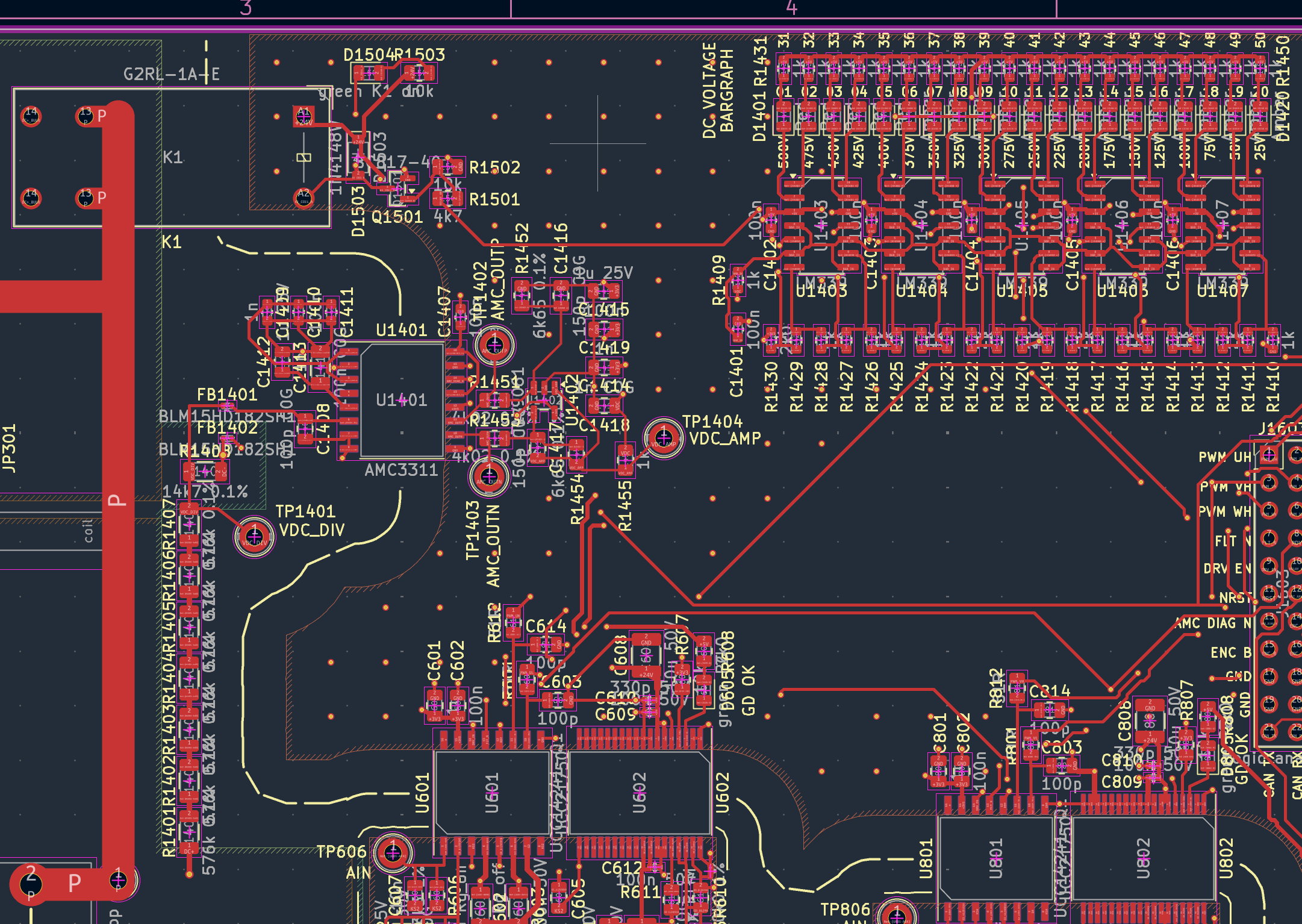
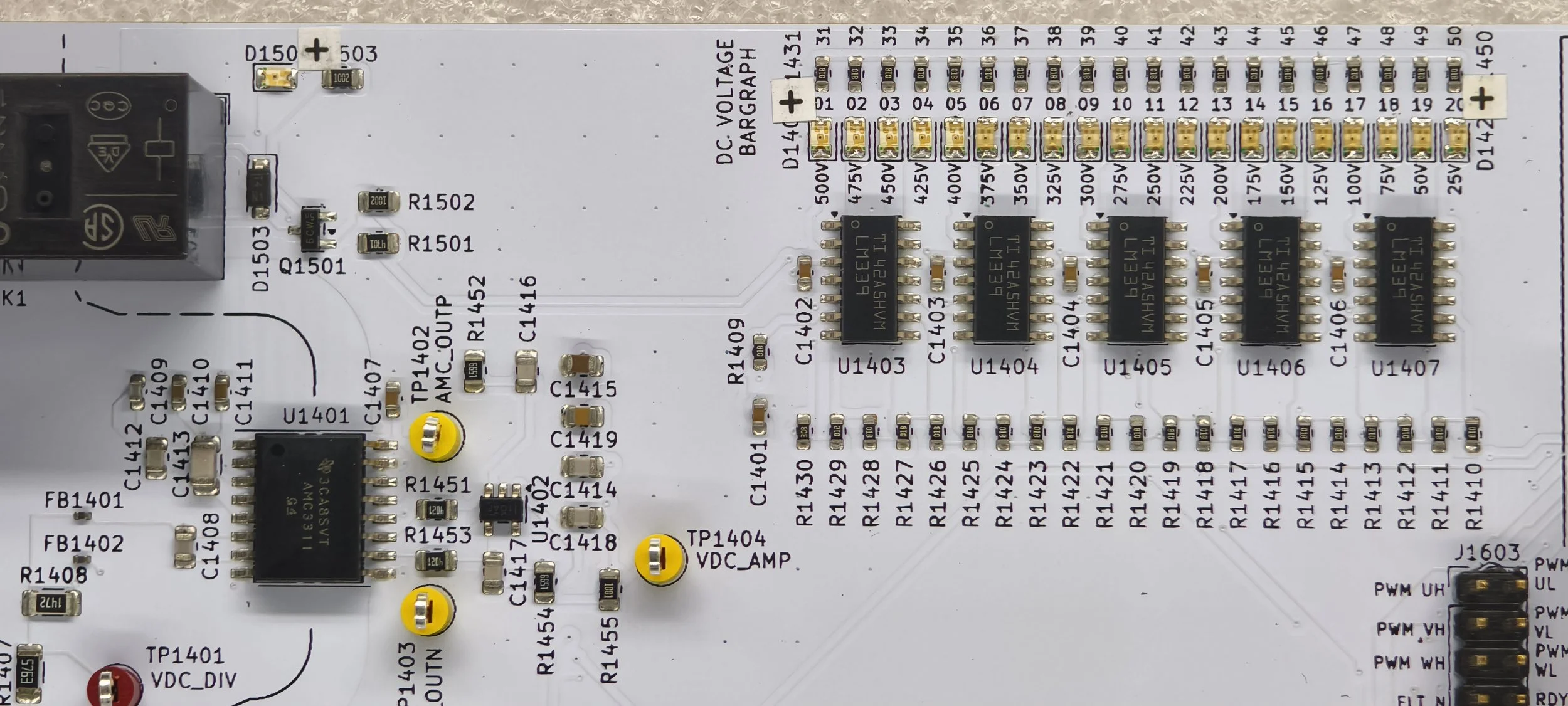
Chain:
resistor divider R1401–R1408 (7 × 576 kΩ + 14.7 kΩ, 0.1 %) from DC+ to DC−
→ AMC3311 isolated amplifier U1401 (gain 1, input 0–2 V, referenced to DC−)
→ difference amplifier U1402 (TLV9061, gain 1.654)
→ 1 kΩ + 1 nF (R1455, C1418)
→ signal VDC to
the 12 bit ADC (0.134 V of DC link per count)≈ 2420 counts,
an STM32 comparator (overvoltage)
and the bargraph.
Divider. TI's method (AMC3311 datasheet SBASAQ5A, 8.2.2):
no unit resistor should see more than 75 V, and about 100 µA should flow.
Seven 576 kΩ resistors (4.03 MΩ) see at most 60 V each at the 420 V trip (79 V at 550 V, which the link never reaches);
14.7 kΩ at the bottom gives 2.0 V at 550 V.
At 358 V the divider draws 88 µA and dissipates 32 mW (4.5 mW per resistor).
With 0.1 % parts the scale is right to about 0.3 % without calibration.
The AMC3311's 1 GΩ input and ±15 nA bias current are negligible against 14.7 kΩ.
AMC3311. Same family as the AMC3301 (isolated DC/DC inside, reinforced barrier), but with a 0–2 V input and
gain 1.
Difference amplifier. VDC = (6.65 kΩ / 4.02 kΩ) × (OUTP − OUTN) = 1.654 × V_in: 6.0 mV per volt of DC link,
the scale the bargraph ladder was designed for (0.150 V per LED = 25 V).
No offset is needed because the voltage is never negative. 150 pF across 6.65 kΩ gives 160 kHz.
Overvoltage trip at 420 V (2.52 V on VDC) through an STM32 comparator: protects the 450 V capacitors, e.g. when the motor feeds energy back while braking (V1 has no brake chopper, so the firmware must limit deceleration).
Failsafe: if the AMC3311 loses its input-side supply, its output goes to −2.5 V and VDC reads 0 V, which looks
like a discharged link. The firmware must check AMC_DIAG_N before trusting VDC. The HV LED D301 works independently.
Test points: TP1401 (divider output; it sits at DC− potential, so measure it against DC− with a differential
probe), TP1402/TP1403 (AMC outputs), TP1404 (op-amp output VDC_AMP); TP1604 at the ADC pin.
Bar Graph
This was fun
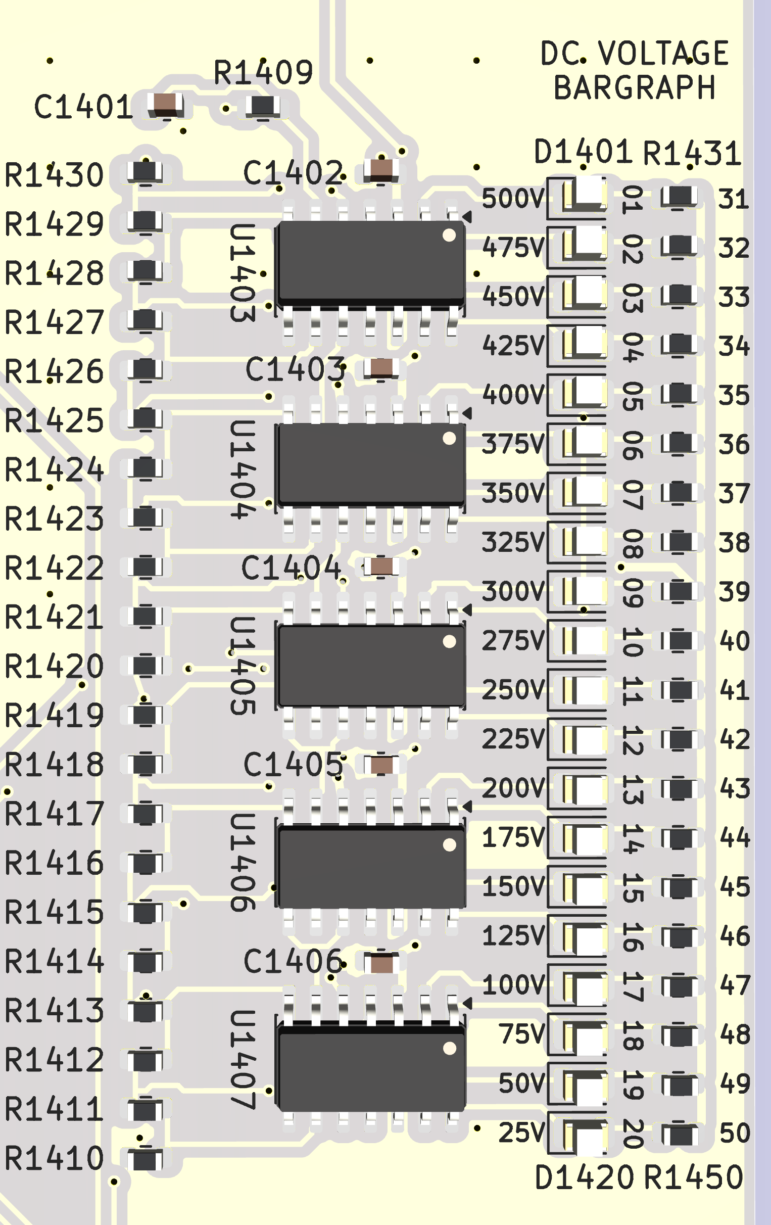
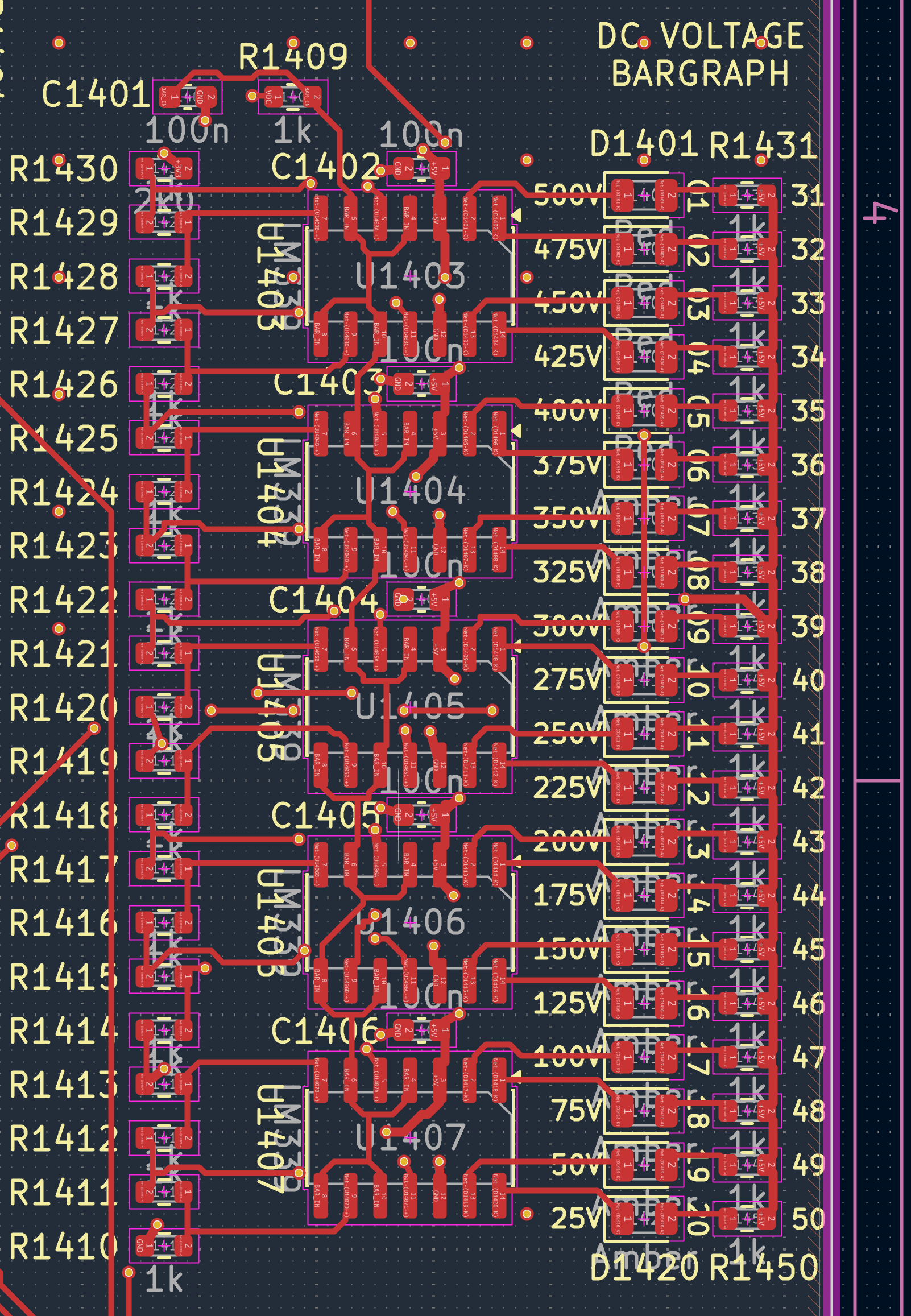
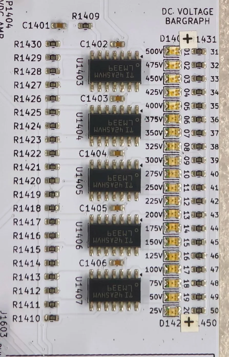
A row of 20 LEDs shows the DC-link voltage in 25 V steps, without any firmware: amber up to 375 V, red from 400 V. It works whenever the 24 V supply is on.
25 V is at the Nucleo side (D1420) and 500 V at the left end (D1401)
the board's vertical text reads from bottom to top, so read that way the bar fills upwards.
A resistor ladder from 3.3 V (R1430 2.0 kΩ, then 20 × 1 kΩ down to R1410 at GND, 150 µA) makes 20 reference voltages TAP_k = (21 − k) × 0.150 V for LED k (D14kk).
Because the VDC signal is 3.3 V at 550 V (6 mV per volt), each step is 25 V of DC link:
D1420 lights at 25 V, D1401 at 500 V.
Five LM339 quad comparators (20 comparators, supplied from 5 V) compare the VDC signal with each tap. When VDC exceeds TAP_k, comparator k pulls its open-collector output low and LED k lights (from 5 V through 1 kΩ: ≈ 2.8 mA).
R1409/C1401 (1 kΩ, 100 nF: 0.1 ms) filter the VDC signal for the comparators: the 100 Hz ripple stays visible and the comparators' switching stays away from the ADC signal. C1402–C1406 decouple the five LM339.
Aux Supply
24 V in, and to the gate driver bias supply, and 5 and 3.3 V to the micro controller circuits
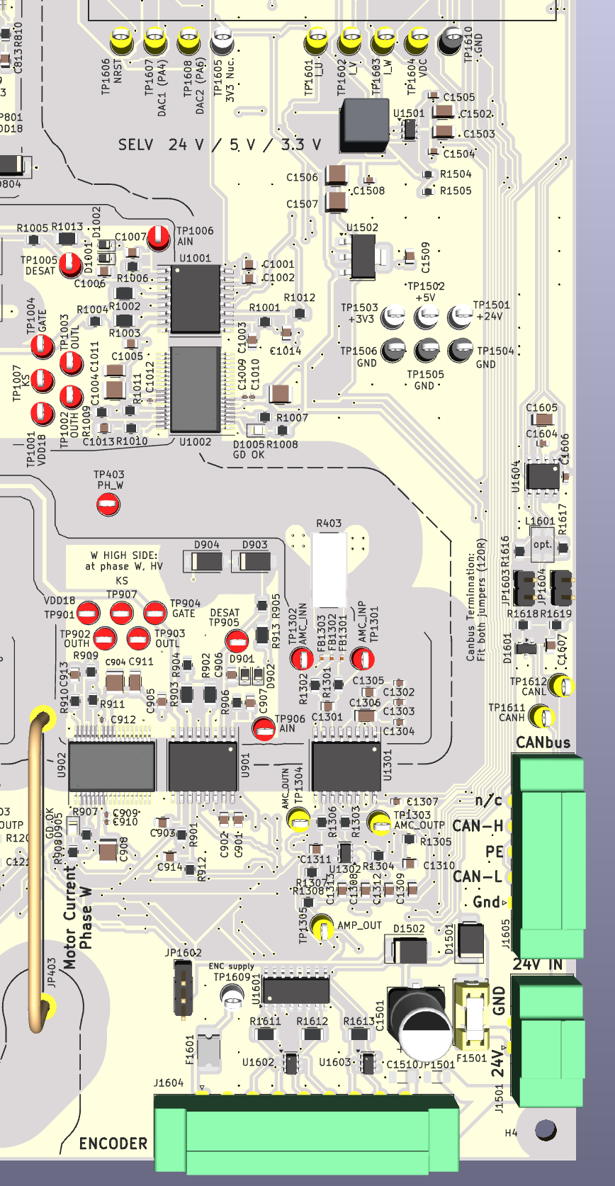
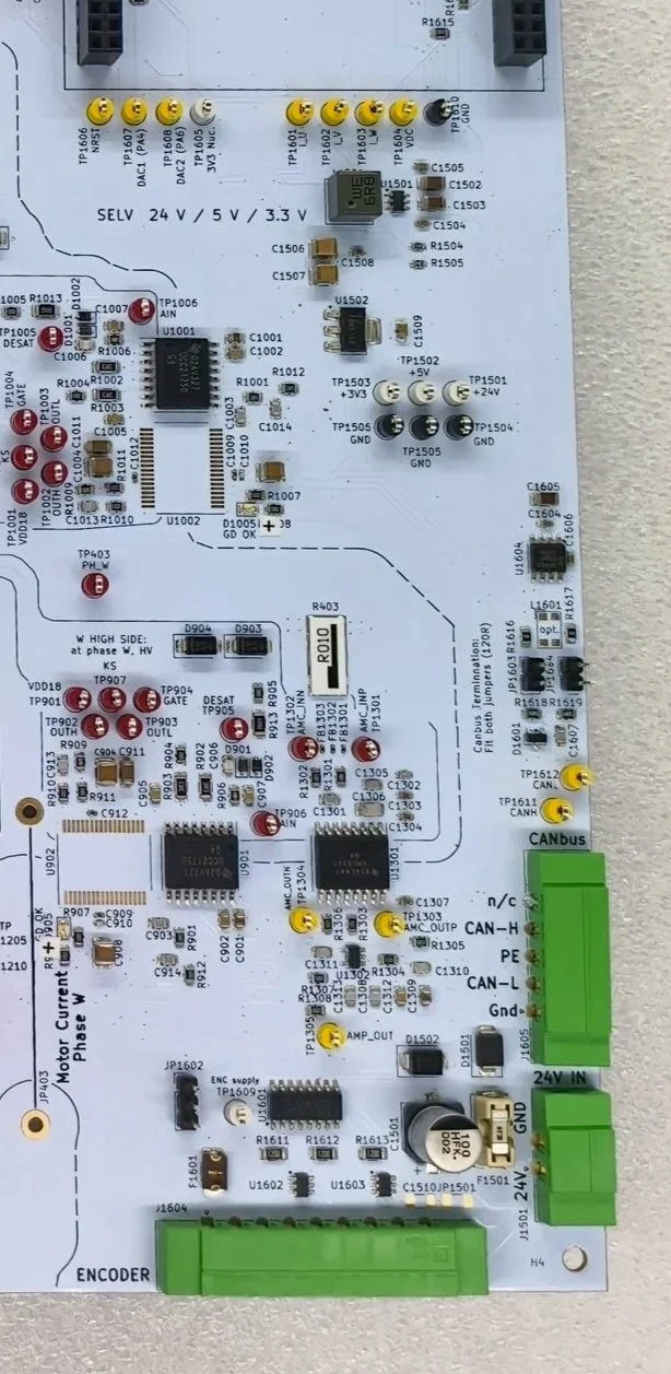
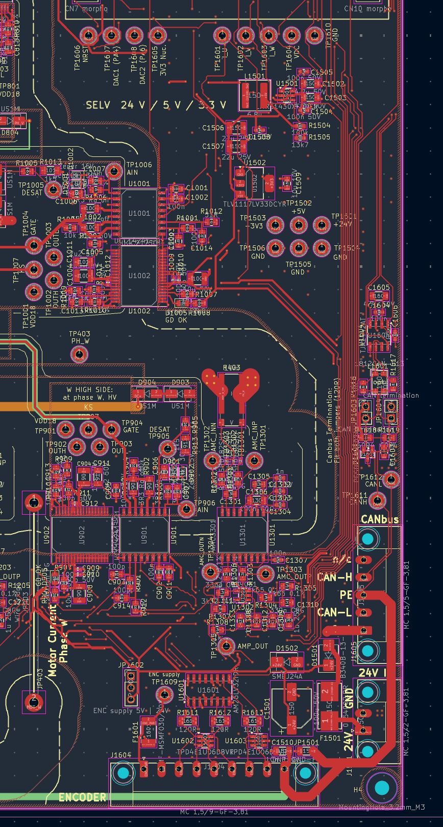
Everything except the power path runs from an external 24 V SELV power supply.
Input chain (J1501 → F1501 → D1501 → D1502 + C1501 → +24V):
J1501: Phoenix Contact MC 1,5/2-GF-3,81 header (1827868) with the MC 1,5/2-STF-3,81 plug
F1501: Littelfuse OMNI-BLOK 154 holder with a Nano2 2 A fast-acting fuse (0154002.DR). Fuse can be replaced without soldering.
D1501: reverse-polarity protection, Schottky diode B340B (40 V, 3 A, SMB). A Schottky diode has a lower forward voltage than an ordinary silicon diode (about 0.4 V at our 0.55 A, 0.2 W).
Surge clamp D1502: SMBJ24A (600 W TVS diode, SMB package). The tightest limit on the 24 V rail is the
bias supply (UCC14241-Q1, and the fitted UCC15241-Q1 alike): 21–27 V in operation, 32 V absolute maximum (above about 31 V it pauses and restarts by itself, which is harmless).Hot-plug damping, C1501 (100 µF 50 V aluminium electrolytic, Panasonic FK, 8 × 10.2 mm): plugging a live 24 V cable into ceramic capacitors makes the cable inductance ring, with peaks up to almost twice the supply voltage and currents of tens of amperes, more than the TVS can hold below 32 V. The electrolytic's internal resistance (a few hundred mΩ) damps the ringing, so the TVS only has to catch smaller spikes such as ESD.
5 V buck converter U1501: TI LMR51430XFDDCR
(4.5–36 V input, 38 V absolute maximum, 3 A, SOT-23-6). A buck converter chops the 24 V with an internal high-side MOSFET at 500 kHz and smooths it with an inductor and capacitors.
The IC also contains the low-side switch (a "synchronous" buck).
3.3 V regulator U1502: TI TLV1117LV33DCYR
(LDO, 1 A, SOT-223, input 2–5.5 V, stable with ceramic capacitors).
An LDO is a linear regulator: it burns the difference between 5 V and 3.3 V as heat. That is fine here because the
current is small, and its output is quieter than a second buck converter would give, which helps the analog circuits.
Nucleo power: the 5 V goes to the Nucleo's E5V pin (CN7 pin 6) with jumper JP5 on pins 5-6.
UM2505 §7.4.1: switch on the 24 V first and then plug in the USB cable. In the other order the Nucleo first runs from the PC's USB port, which may not supply enough current.
SELV ground and PE (JP1501, C1510, both not fitted): the board's GND is not connected to PE.
During bring-up, the USB cable and the scope set the ground potential. JP1501 is a 1206 footprint between GND and PE: fit a 0 Ω resistor to earth the SELV side hard (PELV), or 1 MΩ to drain static charge only.
C1510 (10 nF) is an optional high-frequency bond. Place both near J1501. The reinforced insulation between HV and SELV does not depend on this choice.
Test posts:
TP1501 +24 V,
TP1502 +5 V,
TP1503 +3.3 V,
TP1504–TP1506 GND (short scope ground leads).
Relay driver
K1 coil: Q1501 (Nexperia BC817-40, NPN transistor, 45 V, 500 mA, SOT-23) switches the low side of the coil (net K1_COIL_N) from RELAY_EN.
Micro Controller Interface
Morpho-connectors to the MCB to the left, debug connectors beneath.
To the right is some of the encoder interface.
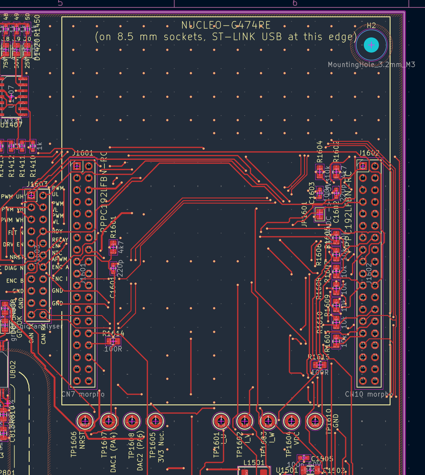
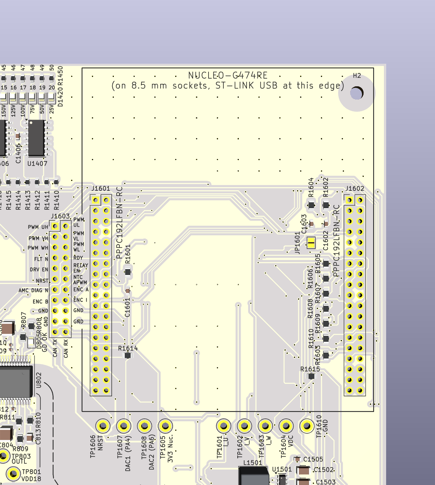
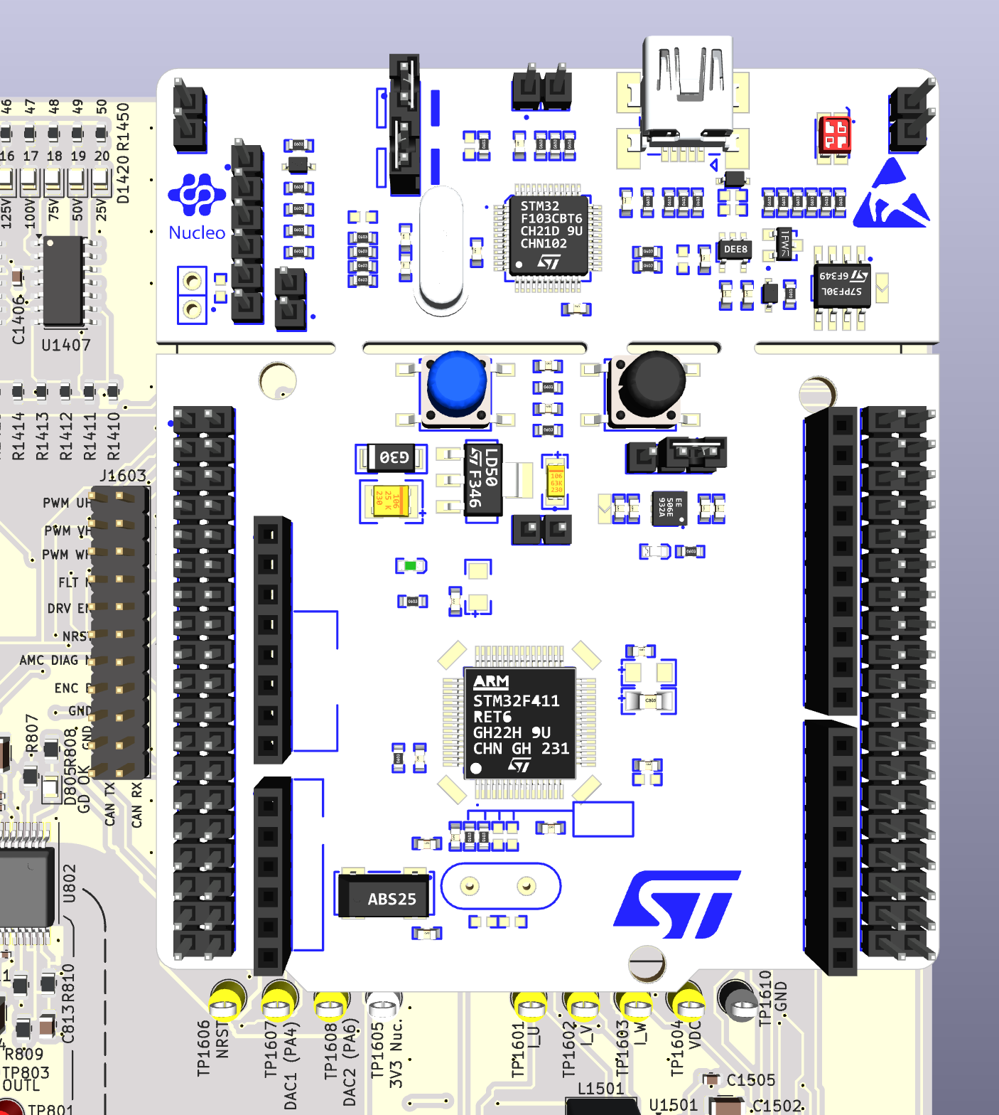
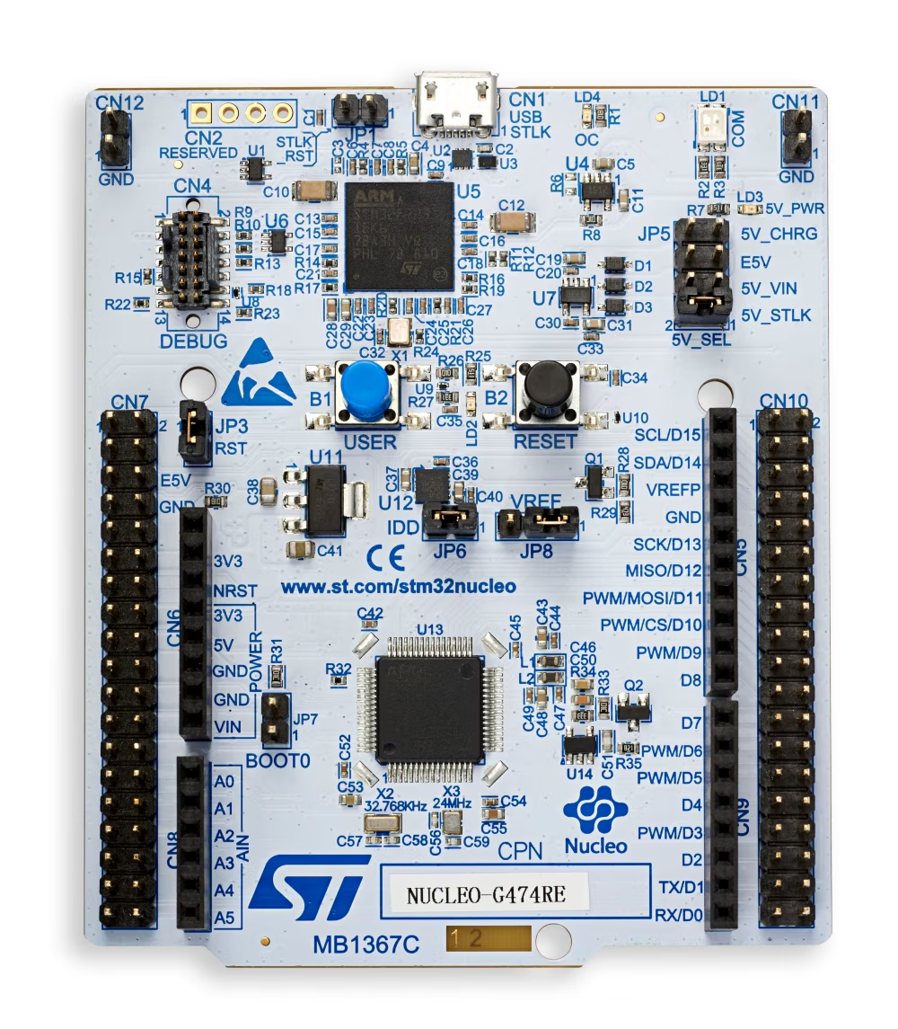
The NUCLEO-G474RE plugs onto two 2 × 19 sockets (J1601 = CN7, J1602 = CN10).
These sockets also works on a NUCLEO-G431RB (with fewer comparators).
Nucleo settings:
Jumper JP5 on 5-6 (power from E5V = the board's +5V) and JP8 on 2-3 (ADC reference VREF+ = the
Nucleo's 3.3 V supply).
PWM: TIM1 CH1/CH2/CH3 on PA8/PA9/PA10 (high sides), CH1N/CH2N/CH3N on PA11/PA12/PB15 (low sides). The dead time is generated in the timer.
R1605–R1610 (10 kΩ) pull every PWM line low while the MCU is in reset. This matters because each PWM also drives the partner driver's IN−, which has an internal pull-up; an undriven line would float.FLT_N → PA15 = TIM1_BKIN.
The six drivers' FLT outputs are open-drain and wired together.
R1601 (4.7 kΩ) pulls the line up and C1601 (220 pF) filters noise.Any driver fault pulls the line low, and the timer's break input switches all six PWMs off in hardware.
PA15 is 5 V tolerant, so the pull-up to the board's +3V3 does no harm while the Nucleo is unpowered.
RDY → PC9 (R1602 4.7 kΩ + C1602 220 pF): all driver supplies are good.
DRV_EN ← PB5: R1603 (10 kΩ) pull-down, so the drivers stay disabled until the firmware enables them.
AMC_DIAG_N → PB9: R1604 (10 kΩ) pull-up. Any of the four isolated amplifiers pulls it low on a fault. The firmware must check it before trusting VDC, because a lost AMC3311 supply reads as 0 V.
RELAY_EN ← PB2 (to the K1 driver on the aux sheet).
Analog inputs, two pins per phase current:
A comparator compares an input pin with a threshold from an internal DAC.
The DAC can only reach the comparator's (−) input, and the (+) inputs are fixed pins.The phase currents swing both ways around 1.65 V, so each phase uses two comparators (high and low limit), and its signal goes to two MCU pins:
I_U → PA1 + PA0, I_V → PA7 + PB11, I_W → PB0 + PB13. VDC → PB14.That uses all seven comparators of the G474.
All of them can stop the PWM through the TIM1 break input, alongside FLT_N.I_U, I_V, I_W and VDC also go to four different ADCs, so all four are sampled at the same instant.
TP1601–TP1604 sit on these nets.
+3.3VADC comes from the Nucleo's VREF+ pin (CN10-7).
The current-sense cells' 1.65 V zero points are made from it, so they follow the ADC reference exactly.No capacitor is placed on this net: with JP8 in its default position the reference is a TL1431 shunt regulator, and such regulators can oscillate with some capacitive loads.
JP1601 (solder jumper, open) can feed the net from the board's +3V3 for bench tests without a Nucleo. Keep it open when a Nucleo is fitted.
NTC_APWM → PB6 = TIM4_CH1 in PWM-input mode (period and duty measured in hardware).
Debug outputs: the DACs on PA4 and PA6 drive test points TP1607/TP1608 through 100 Ω (R1614/R1615). The firmware can put any internal variable (angle, Id, Iq) on the scope next to the real signals. With all seven comparator thresholds active, PA4 shares its DAC with a threshold.
PA6 stays free (G474 only).NRST (the MCU reset) goes to J1603 pin 11 and TP1606: an unexpected reset shows on the logic analyser.
TP1605 is the Nucleo's own 3.3 V, TP1610 a GND post.
Further interface (nice to have):
Encoder interface:
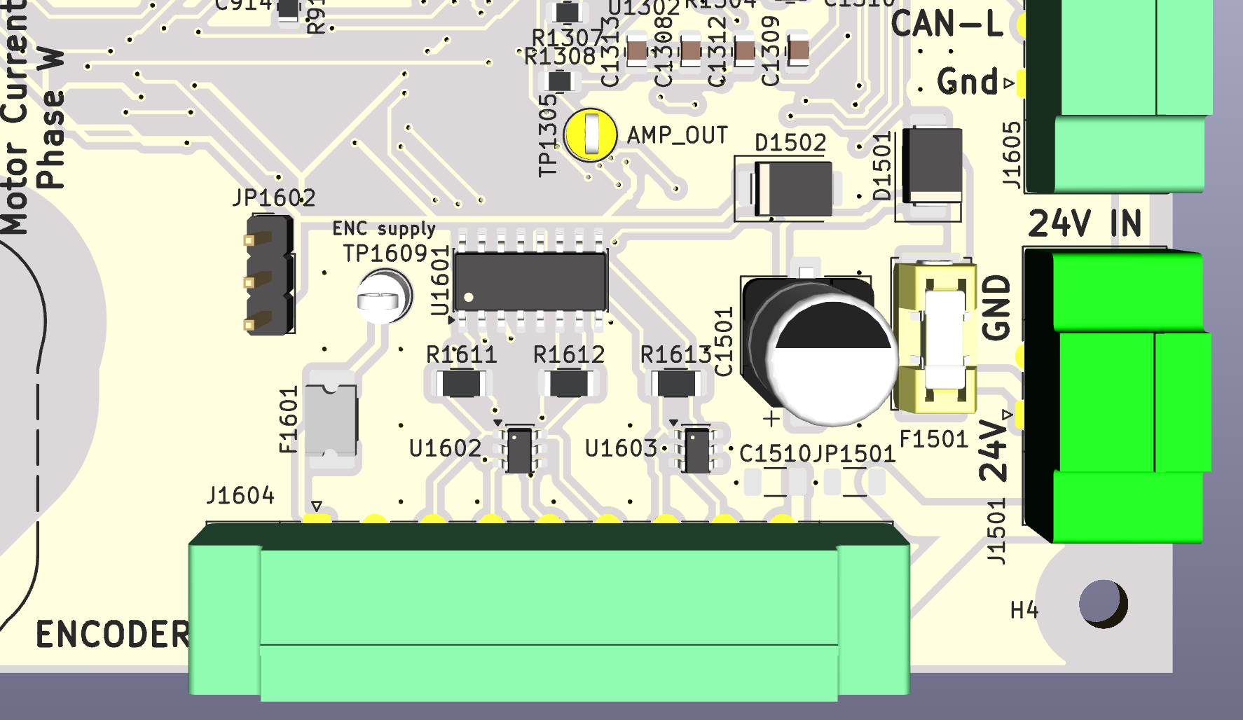
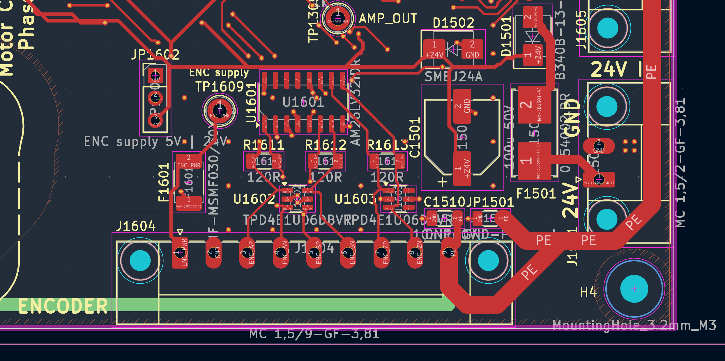
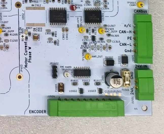
J1604: Phoenix MC 1,5/9-GF-3,81 (9 poles, same family as the 24 V input): 1 supply, 2 0 V, 3/4 A±,
5/6 B±, 7/8 Z±, 9 shield. The shield goes to PE, the usual practice for a drive's encoder cable.Supply: jumper header JP1602 selects +5 V (shunt on 1-2) or +24 V (2-3). With no shunt the encoder gets no supply. A pin header is used instead of a solder jumper because one blob of solder across three pads would short +24 V to +5 V.
F1601 (Bourns MF-MSMF030/60X, resettable, 0.3 A) protects against a short in the cable;
TP1609 = encoder supply.Receiver: U1601 (TI AM26LV32) turns the three differential pairs into 3.3 V logic:
ENC_A/B → PC6/PC7 (TIM3 encoder mode),
ENC_I → PC8 (TIM3_CH3 latches the count at the index).R1611–R1613 (120 Ω) terminate each pair at the receiver end, matching the cable impedance.
An RS-422 line has a single driver, so it is terminated only at the receiving end.U1602/U1603 (TI TPD4E1U06) clamp ESD from the cable on all six lines.
The AM26LV32 is always enabled (G high, G̅ low). Its unused 4th receiver has open inputs.
Only encoders with RS-422 (5 V line-driver) outputs:
HTL encoders (24 V push-pull outputs) would destroy the receiver and the ESD arrays.
CAN bus:
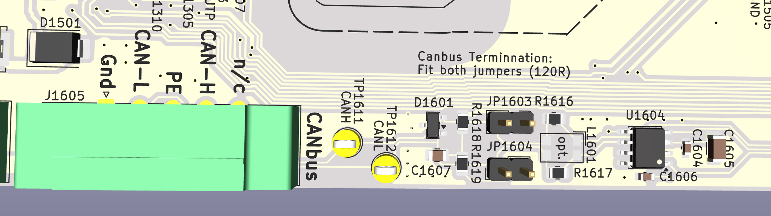
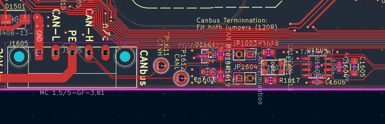
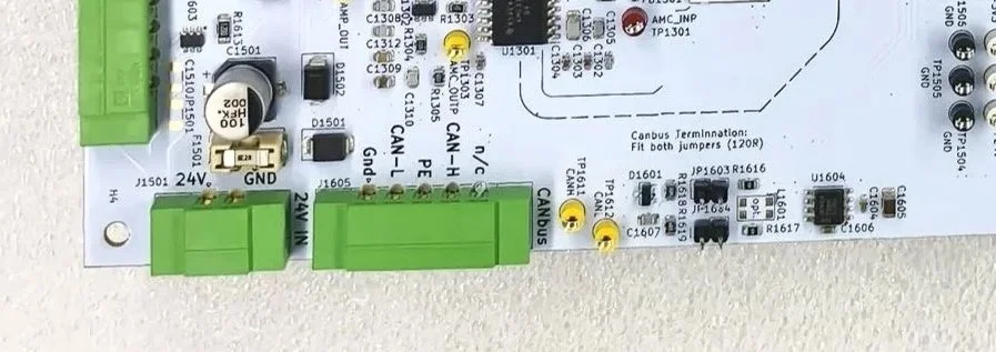
A link to a PC (USB-CAN adapter) or to other CAN nodes.
MCU side: FDCAN3 on PB4 (TX) and PB3 (RX), alternate function AF11.
These pins exist only on the G474 (the G431 has FDCAN1 only, whose pins are taken by the PWM, BOOT0 and AMC_DIAG_N): on a NUCLEO-G431RB the board has no CAN.
PB3 is also the Nucleo's SWO trace pin (solder bridge SB15 to the ST-LINK); SWO is not used.U1604 (NXP TJA1442AT): the transceiver turns the MCU's TX/RX logic signals into the two-wire differential bus and back. The "A" version has a VIO pin: TXD, RXD and STB work at the 3.3 V of VIO (+3V3, C1606), the bus driver runs from +5V (C1604, C1605). Classic CAN and CAN FD up to 5 Mbit/s.
STB (standby) ← PB7.
The pin has an internal pull-up, so while the MCU is in reset or the Nucleo is unplugged the transceiver is in Standby and stays off the bus.
The firmware drives PB7 low to talk. A stuck-low TXD is released by the transceiver after 0.8–9 ms (dominant time-out), so a crashed MCU cannot block the bus.L1601 (Coilcraft 1812CAN-513, 51 µH common-mode choke) is not fitted:
R1616/R1617 (0 Ω) bridge its two windings.
To try the choke in EMC experiments, fit L1601 and remove both 0 Ω resistors.D1601 (Nexperia PESD2CANFD24V, 6 pF) clamps ESD and transients from the cable on both lines; the TJA1442 itself withstands −36/+40 V and 8 kV on CANH/CANL.
Termination: a CAN bus is a line terminated with 120 Ω at both ends (it has many drivers, unlike RS-422).
Here the 120 Ω is split into R1618 + R1619 (2 × 60.4 Ω) with C1607 (4.7 nF C0G) from the midpoint to GND, which also damps common-mode noise.J1605: Phoenix MC 1,5/5-GF-3,81 (5 poles, same family as J1501/J1604), pinning per CiA 303-1 (the open-style connector of CANopen/DeviceNet):
1 CAN_GND,
2 CAN_L,
3 shield (→ PE, as at J1604),
4 CAN_H,
5 CAN_V+ (not connected).
TP1611/TP1612 sit on CANH/CANL; the bus signal is CANH − CANL (≈ 2 V dominant, 0 V recessive).
Grounding: CAN_GND is the board's SELV GND.
Use a galvanically isolated USB-CAN adapter on the PC, so the cable does not tie SELV GND to the PC's earth (the USB cable already does that while it is plugged in).
J1603 logic-analyser header (2 × 11) for the PicoScope MSO's digital inputs:
the six PWMs,
FLT_N,
RDY,
DRV_EN,
RELAY_EN,
NRST,
NTC_APWM,
AMC_DIAG_N and
ENC_A/B/I, four GND pins (17–20), and
CAN_TX/CAN_RX on pins 21/22
(the MSO has 16 digital channels: clip the ones the measurement needs).
Reserved, not connected: SPI3 (PC10–PC12 + PD2), brake PWM (PC3, TIM1_CH4).