Together with the output current measurement, accurate DC-link voltage measurement is of utmost importance.
This post will describe how the sensor is chosen and all the steps required to create a PCB design.
We have earlier stated that we want to separate the two sensing circuits to individual boards so that modifications can be done more easily in the prototyping phase.
Step 1: Requirements and specification
During development the supply voltage will be single phase 230 V AC supply at 50 Hz, but we also want to be able to use three phase 400 V AC, so the nominal DC-link voltage is chosen based on that supply:
\[ V_{DC-link} = V_{supply} \cdot \sqrt{2} = 400 V \cdot \sqrt{2} = 565.7\;V\]
The output of the sensor has to match the range of the analog-to-digital converter (ADC) which is translating the analog value to a digital one used by the FPGA and the processor on the Zync 7000 SoC.
The current controller board is Red Pitaya STEMboard 125-14 which features several ADCs:
- 2x High-speed ADCs at 125 MS/s and 14 bit connected to the external SMA-connector. Two voltage ranges available: ±1 V and ±20 V. The range is chosen by means of jumpers.
- 4x Auxiliary ADCs connected to the extension contact strip E2. 100 kS/s and 12 bits. Voltage range 0 - 3.5 V.
However, it has been decided to select dedicated ADCs on an external PCB in favor of the ones already available on the STEMboard. The reason for this is portability; we want to be able to select a different controller based on Zync 7000 without being bound to the custom rescaling performed on the STEMboard. For instance, the FPGA ADC is originally meant for ±0.5 V, but between the analog input channel on E2-connector and the FPGA, there is a voltage divided network so that the external input has to be scaled for 0-3.5 V.


Step 2: Selection of analog-to-digital converter (ADC)
For a high resolution measurement, the number of bits assigned to the transformed value is important. Our application has to span from zero to well above the nominal DC-link voltage to be able to measure over voltages (which occur each time the motor is braking).
A 12 bit ADC is able to divide the input range in to \(2^{12} = 4096\) different values. This means that if the input voltage range was 0-1000 V, the resolution would be 0.244 V which is excellent in our application.
The actual measurement range is described and chosen in the next step.
The next important property of the ADC is its sample speed. That is, how often it provides new measurements. Typical values ranges from 10 000 samples per second (1 kS/s) to several GS/s.
Because we want to use the same type ADC for both voltage and current measurements, and because current measurements should be fast, we have landed on an ADC with a sample speed of 500 kS/s which is more than sufficient. It also meets the requirement of the current sensors which can supply a maximum of 400 kS/s.
The selected ADC in the package "6 SOT23"
The winner is Maxim MAX11665AUT+
This chip is available in several configurations depending on the number of channels and resolution. The single channel 12-bit edition is delivered in a package referred to as 6 SOT23. I.e. a typical tiny chip with 6 legs as shown in the illustration to the right.
The digital output of the ADC is a serial line which is synchronized to the FPGA by means of a clock signal. This ensures that both the ADC and the FPGA is keeping the same pace.
The type of serial line selected is Serial Peripheral Interface Bus (SPI). The "bus" part of the name indicates that it is possible to attach several ADCs (or other types of components with SPI) to the same line and thus form a "train" of information inside a 3-wire single signal. This will be handy when creating a single PCB with all the ADCs for current and voltage measurements. It is also an industry standard (along with UART and I²C) which makes it very portable should we decide to change any of the components later.
The clock speed of the SPI bus determines how fast the serial line can transmit data. The datasheet reports that 500 kS/s is achieved at 8 MHz clock speed, but if several ADCs are used on the same bus, the time available for each device on the bus is reduced accordingly.
Six devices (as we plan to install on the dedicated ADC board) means 8/6 = 1.33 Mhz effective clock speed and a signal speed of 83.33 kS/s. This limitation can however be circumvented by creating a dedicated SPI bus for each ADC, but requires some FPGA programming.
Step 3: The voltage sensor and measurement range
The actual voltage sensing device is a LEM LV-25 P
Front and back of the LEM LV-25 P voltage sensor
From the data sheet we can see that the primary current, \(I_p\), is 10 mA. External primary measurement resistor \(R_1\) should be dimensioned so that nominal voltage returns about 10 mA through the primary measurement circuit of the sensor. (\(R_1\) will also step the voltage down so that we are well within the maximum insulation voltage of 500 V).
When deciding the voltage measurement range it is important to note that we want to be able to measure overvoltages also. This is especially important during motor braking where energy from the decelerating motor will charge the DC-link capacitor and increase its voltage.
Internal circuit diagram of the voltage sensor
The sensor's maximum measurement current, \(I_{pm}\), is 14 mA, so that 40 % overvoltage is possible before going out of range for the measurement sensor. This is more than suffcient for our application.
Typically, if the voltage level exceeds 110-115%, a braking resistor is engaged from the main DC-link to decrease the voltage. If however, the voltage increases further (indicating failure in either braking resistor or braking chopper), the inverter should trip long before reaching 140 %.
What about the DC-link capacitors? These are crucial to protect because an over voltage can permanently damage them. As we are using two 500 V capacitors in series, their nominal voltage is increased to 1000 V DC which is well above 140 % of 565 V (791 V). So we got them covered. Phew.
To obtain 10 mA at the primary side of the measurement circuit when the applied voltage is 565 V, one refers to Ohm's law:
\[ \frac{565 \;V}{ 10\; mA } = 56569 \;\Omega \]
Subtracting the 220 ohms already in the measurement winding (which we measured using an ohm meter when the sensor arrived), the external resistance needed is about 56400 ohm.
To reduce the power dissipation in \(R_1\), we want to use several in series. If we use for instance six, each of them has to be 9391 ohm.
Using stock resistors, 9391 ohm is not available. Depending on which resistor series you wish to use, the closest we can get is about 9420 ohm in the E192-series. (192 refers to the amount of available values between each decade, e.g. between 100 and 1000).
If we are a cheap however, we can use 10k resistors instead. This will make the nominal DC-link voltage translate to:
\[ \frac{565 \;V} { (6 \cdot 10000 + 220) \;\Omega } = 9.4 \;mA \]
Not too far away from 10 mA, and more than sufficient. Remember, at 230 V line voltage, the measurement current will be 5.4 mA and this will be the most used voltage level during development.
When the nominal value is at 9.39 mA instead of 10 mA, the corresponding maximum voltage level measurable at 14 mA changes from 791 to 843 V.
Back to the power dissipation in the resistors: Using 140 % DC-link voltage at 400 V input as basis, each resistor will have a maximum voltage drop of
\[ 400 \cdot \sqrt{2} \cdot 1.4 = 132\; V\]
which gives the following energy dissipation in each resistor:
\[P = \frac{U^2}{R} = \frac{(132 \;V)^2}{10k \;\Omega} = 1.73 \;W\]
Knowing this, we want to add significant margin and select resistors rated for 5 W to make sure that they are not overheated.
Additionally, remember that these resistors need to withstand very high voltages compared to normal PCB resistors.
Last aspect; accuracy. With an sensor input voltage of 12 to 15 V the data sheet states the accuracy to be ± 0.9% of Vpn, i.e. less than 5 volt. The stability of this accuracy is important; if an inaccurate value of ± 5 V is stable it can be offset by use of potmeter or software to counter or increase the accuracy.
This will be checked with an oscilloscope later in the project.
Step 4: Secondary side scaling
As the input circuit has been accounted for, we move to the output circuit of the measurement sensor. We now have to scale the output to match the ADC input.
From the diagram shown above and the datasheet, we get that the output current is 25 mA when the input current is 10 mA.
This can be translated to voltage by attaching a resistor, \(R_m\), between the output and ground, and measure the voltage drop of the resistor.
As the ADC input range is 0-5 V, we want to scale the measured DC-link voltage so that 0-843 V translates to 0-5 V. We thus want 14 mA output from sensor to be 5 V, using Ohm's law we see that a 357 ohm resistor is needed. This value is available in both E96 and E192 series resistors. Nice!
But, the voltage sensor's datasheet clearly states that the maximum recommended output resistor value should be 190 Ω, so bad luck there.
A 100 Ω is used instead, and the maximum voltage drop of the measurement resistor is will be 3.5 V. This value can be rescaled using an operational amplifier (op-amp) which we will take a look at next.
Step 5: Signal conditioning and offset
In order to control the offset and scaling of the output resistor, an opamp and two potmeters are used. This allows us to take account of all kinds of accuracy errors and tune the output to suit the ADC.
A negative signal-input with negative feedback from the opamp output allows us to amplify the signal and a positive input used with a potmeter makes it possible to alter the signal bias.
The three main parts of the signal path is shown in the schematic below:
The signal path from left to right:
Main voltage connection, step-down resistors, voltage sensor (U1), measurement resistor, opamp with potmeter for bias and scaling. The last plug is the output to ADC.
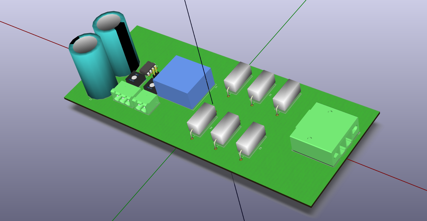
Step 6: Power supply
The PCBs voltage supply with filter capacitors.
Both the opamp and the voltage sensor requires 15 VDC supply, so this has to be supplied from the dedicated power supply card. Still, in order to filter various kinds of noise, we should add a few capacitors as filters.
As we have +15 and -15 V supply, both needs capacitors to ground. Two types of capacitors are used in parallel:
- Electrolyte capacitors, with high capacitance which is preferable for low frequency noise filtering. Note that this type of capacitors have polarity, and must be installed accordingly.
- Ceramic capacitors with lower capacitance but also lower Equivalent Series Resistance (ESR) and Equivalent Series Inductance (ESL) which are better at high frequency noise.
Step 7: Drawing the schematics
As we now know what to do, we get to work. If you do not already have an Electronic Design Automation software (EDA) installed, you can download KiCad which we use here at Switchcraft. It is free, open sourced and supported by CERN.
This post will not go into how to use KiCad (there are dozens of splendid guides out there), so if you have never ever used it before, reserve a few hours to play around with it. Eirik, the co-writer of this blog, taught me how to use it in about 30 minutes, the rest is learnt by playing around and pressing buttons you don't know what do.
Anyway, the described functionality is drawn into a single sheet and shown below:
Full schematic of the voltage sensing card. The opamp in the lower left corner is the second opamp in the opamp chip which is not in use.
When the schematic is complete, there are two more formalities we have to perform before jumping into the PCB layout:
- Assign footprints to each component (i.e. what kind of resistor is R1? What is the pin placement of the voltage sensor?) Most of this is either pick and choose or you will sometime have to design the footprint yourself. It is not particularly difficult or time consuming, and all datasheets have information about footprint dimensions and pins.
- Create at NET list. The NET list describes where each pin is connected. A "NET" is simply all points in the circuit which is at the same potential at all time. In KiCad the program Pcbnew is already embedded and does this for you. It will save a file which the PCB program loads to determine how things are connected.
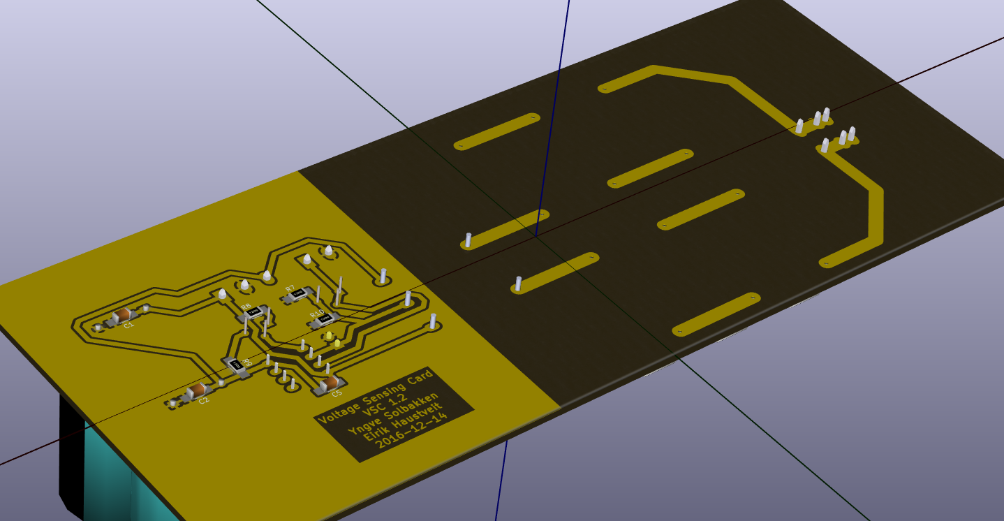
Step 8: Laying the PCB
This is the fun part.
Especially if you enjoy turning your brain inside out while solving Chinese puzzles. Again, I will not go into exactly how the PCB layout program works (it is a part of KiCad), but show you the final results.
The PCB program reads the NET-list you created and basically throws all footprints out on a big pile for you to sort out. There is also an option to spread the components out so that they are not all placed on top of each other, but there is still some work to align all components and draw the paths between each pin.
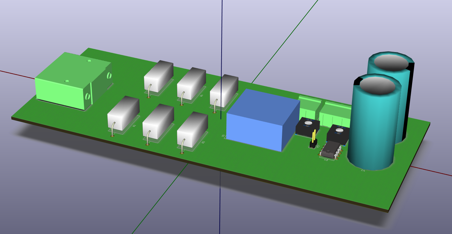
KiCad also features a 3D-viewer, so if you have a 3D model of each component (most are already included, if not it is possible to find models online and import them. I did that for the voltage sensor)
It is very satisfying to inspect your work in full 3D after hours of nitpicking and screwing around with traces and placement.