
It has been some time since last update. The main reason being that I switched job after January 1st this year, and that my new job comes with a great deal of work load and without my 4 week on/4 week off job rotation I had at my previous employer.
My last post concerned the inverter and rectifier card and how they were produced.
Since then I have found that the card's layout was suboptimal at a few points:
- The capacitors were too far away from the transistors, causing unwanted inductance.
- The current sensor board are now included on the inverter card, and the current sensors has been changed to a different type.
- DC-link Voltage sensing is also placed on the board
Creating a new schematic was fairly straight forward. My current challenge is redesigning the PCB layout. We still want to keep the PCB at two levels (front and back) with regards to traces, but this makes it more complicated to add more components, especially as some traces are for the main power (10-20 amps).
Below is how the schematic looks like:
The inverter card schematic: Power electronics on the top, transistor on the lower left, current sensors in the middle and 5V power supply in the lower right corner.
Below is how the current PCB layout looks. This is something like start-over-from-scratch attempt #7, so component placing is not close to final. The goal is to keep the main power electronics (DC-link capacitors, snubber and transistor) on one side of the board with low inductance and low resistance traces. Preferably the DC+ and DC-levels should be large zones instead of conventional traces in order to keep stray inductance to a minimum.
All the other components should be tucked away elsewhere.
Purple-framed components are on one side of the PCB while the green-framed components are on the reverse side. The white lines are where there should be electrical connections (routes). The component placement is not final.
The white lines going all over the place is called a "rats net", and show how every thing should be connected. These are helpful when placing components so that you can arrange them with as short routes as possible.
A few hours has passed since last writing here, and below are the current status of the PCB:

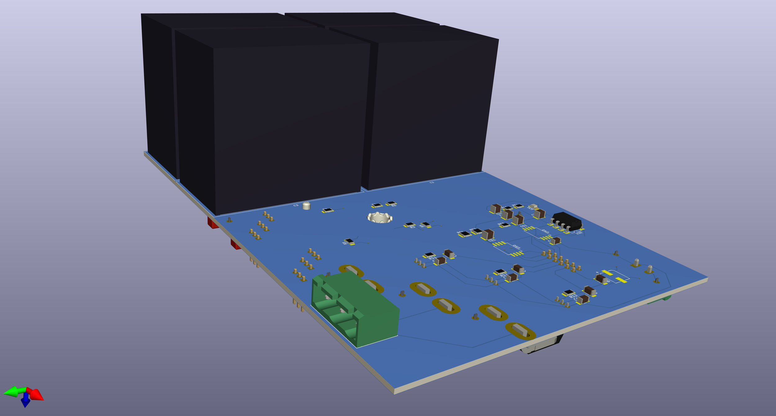

Note that this is still just sketches. The real traces will be drawn up later and the current one are just for testing to see if this design are viable or not.
I'll keep you guys posted